Semiconductor memory device

a memory device and semiconductor technology, applied in the field of semiconductor memory devices, can solve the problem that excellent retention characteristics cannot be maintained specifically in low power supply, and achieve the effect of expanding the operation voltage margin in writing data and excellent retention characteristics

Inactive Publication Date: 2008-04-24
SOCIONEXT INC
View PDF11 Cites 1 Cited by
  • Summary
  • Abstract
  • Description
  • Claims
  • Application Information

AI Technical Summary

Benefits of technology

[0007]It is therefore an object of the present invention to expand an operating voltage margin in writing data while maintaining excellent retention characteristics of a semiconductor memory device.
[0011]When the first storage node holds the “H” level and the second storage node holds the “L” level, the storage node voltage control circuit performs control so that in writing data into the latch circuit, the voltage at the second storage node is raised. Thus, a gate-source voltage in the first load transistor is reduced and an equivalent resistance thereof is increased, so that the voltage of the first node is readily reversed to the “L” level. In contrast, when the first storage node holds the “L” level and the second storage node holds the “H” level, the storage node voltage control circuit performs control so that in writing data into the latch circuit, the voltage at the first storage node is raised. Thus, a gate-source voltage in the second load transistor is reduced and an equivalent resistance thereof is increased, so that the voltage at the second storage node is readily reversed to the “L” level. Accordingly, in either one of the above-described cases, reverse of storage data in the latch circuit is readily performed, so that an operation voltage margin in writing data is expanded. Furthermore, the power supply voltage applied to each of the sources of the first and second load transistors is not changed. Therefore, excellent retention characteristics can be maintained.

Problems solved by technology

I have found that excellent retention characteristics cannot be maintained specifically in a low power supply voltage.

Method used


Image

  • Semiconductor memory device
  • Semiconductor memory device
  • Semiconductor memory device

Examples


Embodiment Construction

[0019]Hereafter, embodiments of the present invention will be described in detail with reference to the accompanying drawings.

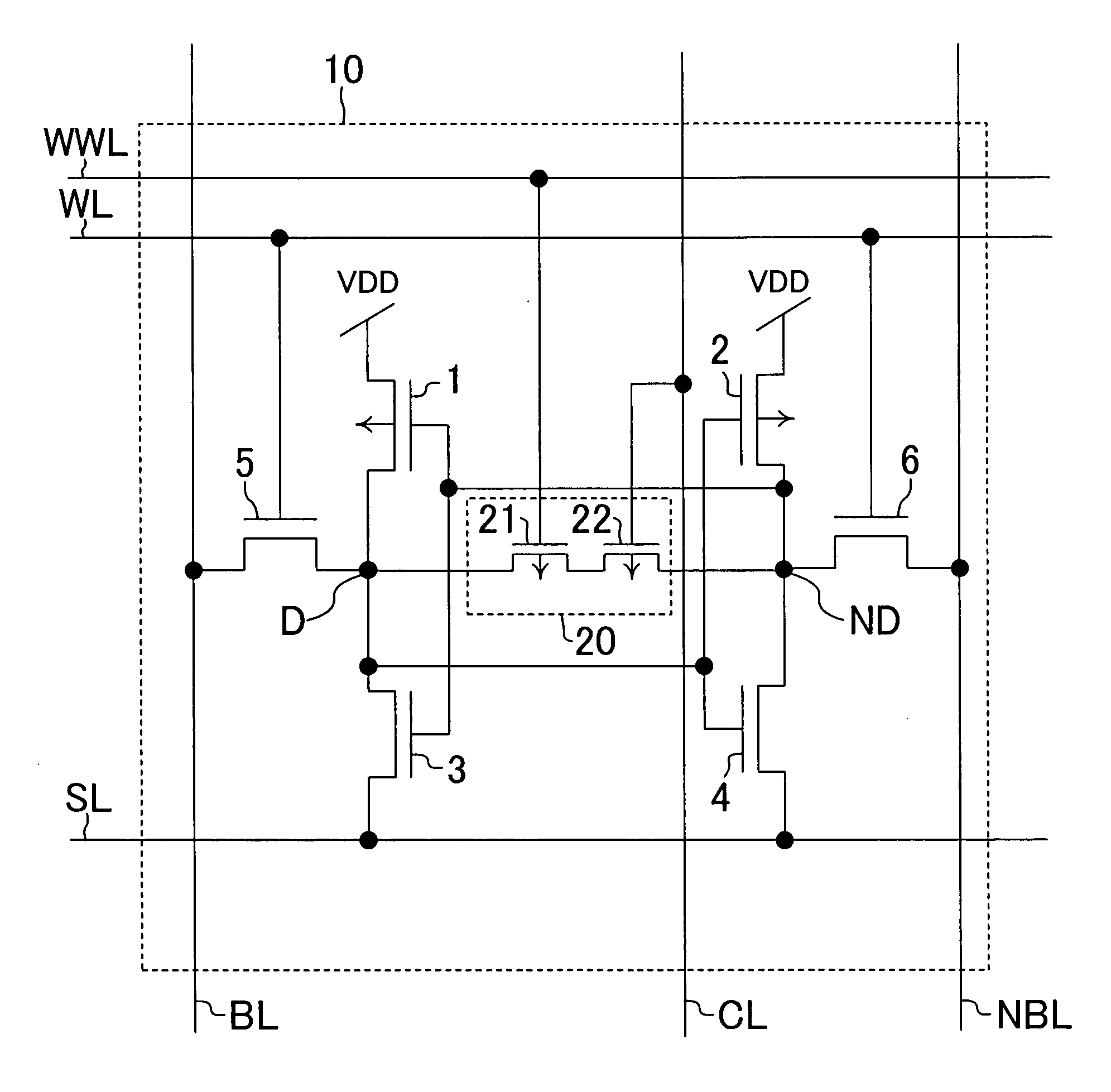
[0020]FIG. 1 is a circuit diagram illustrating an exemplary configuration of a memory cell in an SRAM which is a semiconductor memory device according to the present invention. A memory cell 10 of FIG. 1 is a memory cell for storing complementary data in first and second storage nodes D and DN and includes first and second load transistors 1 and 2, first and second drive transistors 3 and 4, first and second access transistors 5 and 6 and a storage node voltage control circuit 20.

[0021]More specifically, the first load transistor 1 is a p-channel MOS transistor having a drain connected to a first storage node D, a source to which a power supply voltage VDD is supplied and a gate connected to the second storage node ND. The second load transistor 2 is a p-channel MOS transistor having a drain connected to the second storage node ND, a source to which the power...


PUM


Abstract

A storage node voltage control circuit is added to a memory cell including two load transistors, two drive transistors and two access transistors. The storage node voltage control circuit performs control so that in writing data into the memory cell, a voltage at one of the two storage nodes holding a low logic level is raised without changing voltages at respective sources of the load transistors.

Description

BACKGROUND OF THE INVENTION[0001]The present invention relates to a semiconductor memory device including a latch circuit for storing complementary data at two storage nodes.[0002]There has been known a latch circuit in which an output of a first inverter is connected to an input of a second inverter and an output of the second inverter is connected to an input of the first inverter. Each of respective output nodes of the inverters forms a storage node. When each of the inverters has a CMOS structure, a CMOS latch circuit is obtained.[0003]An SRAM memory cell having a 6-transistor structure utilizes the CMOS latch circuit and includes two load transistors, two drive transistors and two access transistors.[0004]According to the techniques disclosed in U.S. Pat. No. 6,316,812 and Japanese Laid-Open Publication No. 2002-42476, to expand a power supply voltage range in which an SRAM memory cell can be operated, a voltage drop element is inserted between a supply line of a power supply v...

Claims


Application Information

Patent Timeline
Patent Type & Authority Applications(United States)
IPC IPC(8): G11C11/00
CPCG11C11/419G11C11/412
Inventor MASUO, AKIRA
Owner SOCIONEXT INC
Why Eureka
Try Eureka