Sputtering of thermally resistive materials including metal chalcogenides

a technology of chalcogenide and sputtering, which is applied in the direction of sputtering coating, vacuum evaporation coating, coating, etc., can solve the problems of reducing the uniformity of sputtering, increasing the heat of the target, and increasing the target power, so as to reduce the thermal load and low thermal conductivity

Active Publication Date: 2008-05-01
APPLIED MATERIALS INC
View PDF11 Cites 58 Cited by
  • Summary
  • Abstract
  • Description
  • Claims
  • Application Information

AI Technical Summary

Benefits of technology

[0009]Metal chalcogenide targets are preferably sputtered with a bipolar pulse form in which a reversed positive voltage is applied to the target with a duty cycle of less than 50% and with a repetition rate of 10 to 200 kHz while the longer negative pulse effects sputtering of the target. Exemplary values are positive pulse widths of 3 microseconds and a 25 to 100 kHz pulse rate. A pulse width of less than about 10 microseconds allows the sputtering plasma to be sustained during the positive pulse. The reversed pulsing is useful in cleaning the target and reducing the thermal load in view of the low thermal conductivity and granular multi-component composition of metal chalcogenide targets.

Problems solved by technology

DC magnetron sputtering typically generates much heat in the target and high target power further increases the heat.
In general, materials other than highly conductive metals poorly conduct heat and thus are subject to excessive heating in conventional sputtering, which may lead to target degradation including cracking.
Non-catastrophic effects include a strong temperature profile across the target, which may degrade sputtering uniformity.

Method used


Image

  • Sputtering of thermally resistive materials including metal chalcogenides
  • Sputtering of thermally resistive materials including metal chalcogenides
  • Sputtering of thermally resistive materials including metal chalcogenides

Examples


Embodiment Construction

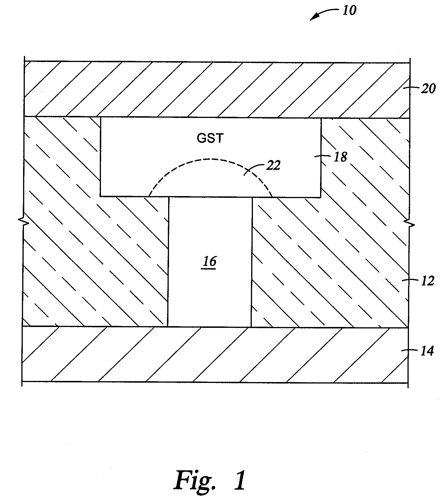
[0019]An example of a phase-change memory (PCM) cell 10 is illustrated in the cross-sectional view of FIG. 1 although the invention is not limited to such a structure. A dielectric layer 12, for example, of silicon oxide, is grown over a bottom electrode 14. A vertical structure is etched through the dielectric layer 12. A via 16 in the lower portion is filled with a metal to contact the bottom electrode 14. A wider plug 18 at the top of the dielectric layer 16 and contacting and overhanging the via 16 is filled with a phase-change material, such as the metal chalcogenide germanium antimony telluride (GST). A top electrode is 20 is deposited over the GST plug 18.

[0020]In operation, a short electrical pulse is applied through the electrodes 14, 20 to the GST plug 18 to cause a phase-change region 22 to melt. The remainder of the GST plug 18 is preferably always in the conductive crystalline state. Depending on whether the melting pulse is short or long, the phase-change region 22 eit...


PUM

PropertyMeasurementUnit
temperatureaaaaaaaaaa

Abstract

A plasma sputtering method for metal chalcogenides, such as germanium antimony telluride (GST), useful in forming phase-change memories. The substrate is held at a selected temperature at which the material deposits in either an amorphous or crystalline form. GST has a low-temperature amorphous range and a high-temperature crystalline range separated by a transition band of 105-120° C. Bipolar pulsed sputtering with less than 50% positive pulses of less than 10:s pulse width cleans the target while maintain the sputtering plasma. The temperature of chamber shields is maintained at a temperature favoring crystalline deposition or they may be coated with arc-spray aluminum or with crystallographically aligned copper or aluminum.

Description

FIELD OF THE INVENTION[0001]The invention relates generally to sputtering of materials. In particular, the invention relates to metal chalcogenides.BACKGROUND ART[0002]Sputtering, alternatively called physical vapor deposition (PVD), is the most prevalent method of depositing layers of metals and related materials in the fabrication of semiconductor integrated circuits. The most commonly practiced form of sputtering is DC magnetron sputtering in which a negative DC voltage is applied to a metallic target in opposition to a grounded chamber shield. A magnetron positioned in back of the target projects a magnetic field adjacent the front face of the biased target to create a high-density plasma of a sputter working gas such as argon. The argon ions of the plasma efficiently sputter metal atoms from the target.[0003]Much of modern sputtering is based on ionizing a large fraction of the sputtered atoms. A high ionization fraction may be accomplished by a small strong magnetron, which in...

Claims


Application Information

Patent Timeline
Patent Type & Authority Applications(United States)
IPC IPC(8): C23C14/35
CPCC23C14/0623C23C14/541C23C14/351
Inventor YE, MENGQIMILLER, KEITH A.DING, PEIJUNYOSHIDOME, GOICHITAO, RONG
Owner APPLIED MATERIALS INC
Why Eureka
Try Eureka