Wafer-level fabrication of lidded chips with electrodeposited dielectric coating

a technology of dielectric coating and lidded chips, which is applied in the direction of semiconductor devices, semiconductor/solid-state device details, electrical apparatus, etc., can solve the problems of low cost, low cost, and low cost of mass-produced chips such as drams

Active Publication Date: 2008-05-01
INVENSAS CORP +1
View PDF22 Cites 188 Cited by
  • Summary
  • Abstract
  • Description
  • Claims
  • Application Information

AI Technical Summary

Benefits of technology

[0017]In accordance with one or more preferred aspects of the invention, the semiconductor element may be ground from the rear face to reduce the thickness of the semiconductor element prior to forming the plurality of openings.

Problems solved by technology

Because such devices are often exposed at a front face of the microelectronic devices, they usually require protection from the elements, such as dust, other particles, contaminants and / or humidity.
Certain types of mass-produced chips such as DRAMs also require packaging costs to be tightly controlled.
Heretofore, wafer-level packaging processes have not been available for fabricating chips having pin-grid array interfaces or compliant ball-grid array (“BGA”) interfaces which keep costs low while also incorporating controlled impedance transmission lines for high-speed performance.

Method used


Image

  • Wafer-level fabrication of lidded chips with electrodeposited dielectric coating
  • Wafer-level fabrication of lidded chips with electrodeposited dielectric coating
  • Wafer-level fabrication of lidded chips with electrodeposited dielectric coating

Examples


Embodiment Construction

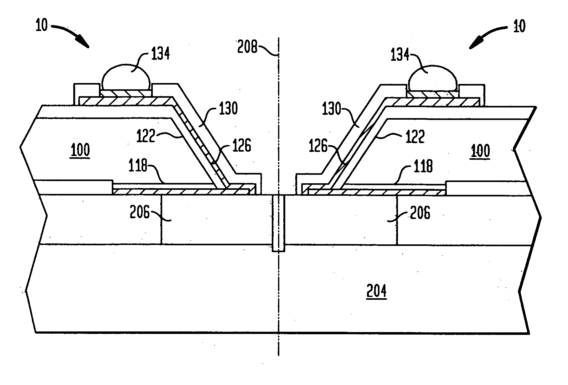
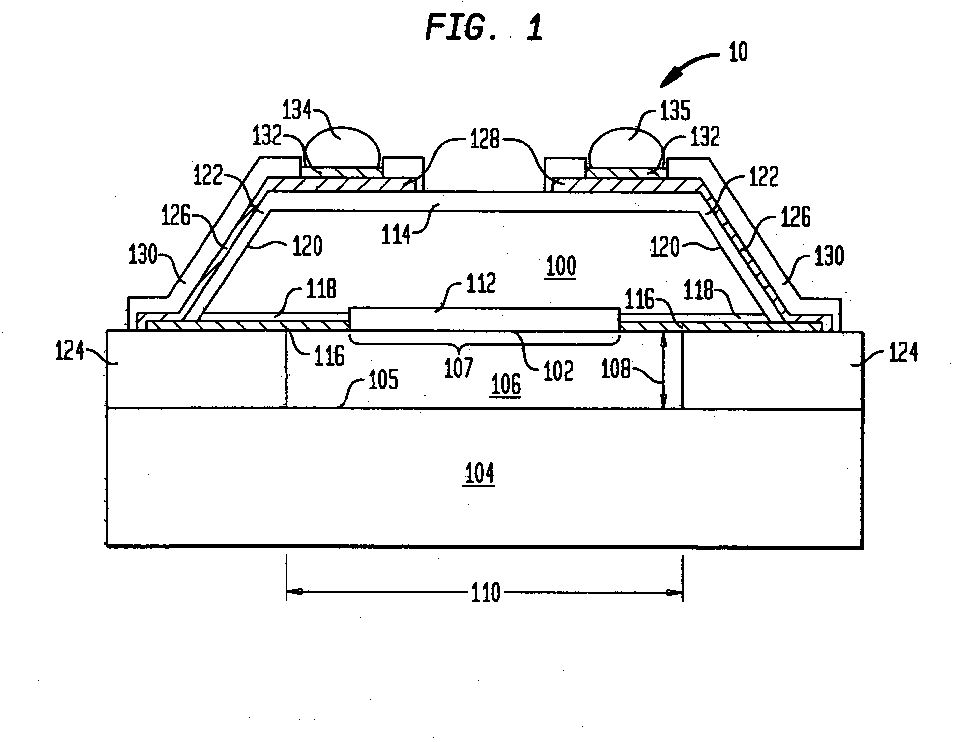
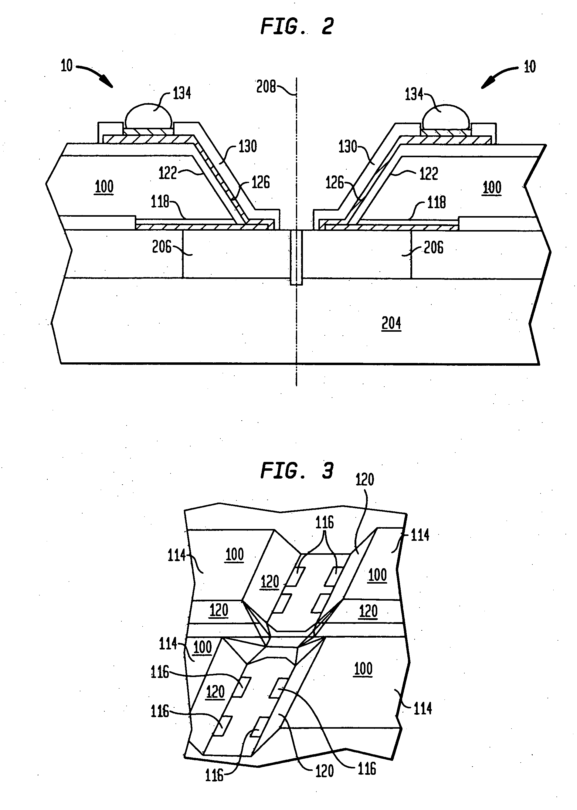
[0054]FIG. 1 is a sectional view of a packaged semiconductor chip 10 in accordance with an embodiment of the invention. As illustrated in FIG. 1, the packaged chip is shown in an orientation in which a front face 102 of the semiconductor chip faces downwardly. As illustrated in FIG. 1, the packaged chip includes a semiconductor chip 100 having a front face 102 and a rear face 114 remote from the front face. The front face of the chip 100 is covered by a lid or cover 104 which is assembled together with the semiconductor chip 100 to form the packaged chip 10. As illustrated in FIG. 1, the front face 102 of the semiconductor chip 100 is oriented downwardly towards an upwardly facing inner surface 105 of the lid 104. The semiconductor chip 100 typically includes a semiconductor substrate in which one or a plurality of semiconductor devices 112 are disposed in a device region thereof below the front face 102. The semiconductor chip 100 also includes a plurality of dielectric layers over...


PUM


Abstract

A method is provided for fabricating a unit including a semiconductor element such as a sensor unit, e.g., for optical imaging. A semiconductor element has plurality of conductive features exposed at the front surface and semiconductive or conductive material exposed at least one of the front and rear surfaces. At least some of the conductive features are insulated from the exposed semiconductive or conductive material. By electrodeposition, an insulative layer is formed to overlie the at least one of exposed semiconductive material or conductive material. Subsequently, a plurality of conductive contacts and a plurality of conductive traces are formed overlying the electrodeposited insulative layer, the conductive traces connecting the conductive features to the conductive contacts. The unit can be incorporated in a camera module having an optical element in registration with an imaging area of the semiconductor element.

Description

BACKGROUND OF THE INVENTION[0001]The present invention relates to packaging of microelectronic devices, especially the packaging of semiconductor devices.[0002]Certain types of microelectronic devices and semiconductor chips include devices such as acoustic transducers, radio frequency emitters and / or detectors and / or optoelectronic devices. Such devices typically require packaging which permits the passage of energy, e.g., acoustic, radio frequency or optical wavelength energy to and from devices at a face of a semiconductor chip.[0003]Because such devices are often exposed at a front face of the microelectronic devices, they usually require protection from the elements, such as dust, other particles, contaminants and / or humidity. For this reason, it is advantageous to assemble the microelectronic device with a lid or other element covering the front face of such microelectronic device at an early stage of processing.[0004]Other types of microelectronic devices require ease of test...

Claims


Application Information

Patent Timeline
Patent Type & Authority Applications(United States)
IPC IPC(8): H01L23/02
CPCH01L2924/30107H01L2924/3011H01L2924/07811H01L2224/11334H01L2924/10253H01L23/3114H01L24/06H01L24/11H01L24/12H01L24/16H01L24/48H01L24/94H01L27/14618H01L27/14683H01L31/0203H01L31/0232H01L2224/0401H01L2224/04042H01L2224/06136H01L2224/114H01L2224/1147H01L2224/116H01L2224/13022H01L2224/13099H01L2224/13147H01L2224/13155H01L2224/274H01L2924/01005H01L2924/01013H01L2924/01014H01L2924/01015H01L2924/01022H01L2924/01027H01L2924/01029H01L2924/01033H01L2924/01046H01L2924/0105H01L2924/01057H01L2924/01078H01L2924/01079H01L2924/01082H01L2924/01322H01L2924/014H01L2924/12044H01L2924/19041H01L2924/19042H01L2924/30105H01L2224/13111H01L2924/01006H01L2924/01023H01L2224/48H01L2224/024H01L2224/0236H01L2924/00H01L31/02325H01L2924/00014H01L2924/351H01L2224/45099H01L2224/45015H01L2924/207
Inventor OGANESIAN, VAGEOVRUTSKY, DAVIDROSENSTEIN, CHARLESHABA, BELGACEMHUMPSTON, GILES
Owner INVENSAS CORP
Why Eureka
Try Eureka