Mask etch plasma reactor with cathode providing a uniform distribution of etch rate

a plasma reactor and cathode technology, applied in the direction of electric discharge lamps, chemical/physical/physicochemical processes, chemical apparatus and processes, etc., can solve the problems of non-uniform e-beam written photoresist patterns, high mask etch cost, etc., to reduce rf non-uniformities and improve conductivity. uniform

Active Publication Date: 2008-05-01
APPLIED MATERIALS INC
View PDF71 Cites 136 Cited by
  • Summary
  • Abstract
  • Description
  • Claims
  • Application Information

AI Technical Summary

Benefits of technology

[0006]In another aspect, the cathode and an underlying facilities plate are formed of a metal. The cathode has a bottom surface and the facilities plate has a top surface facing the bottom surface of the cathode, and they are fastened together by screws of a dissimilar metal. In order to reduce RF non-uniformities at the screw heads, a thin ring

Problems solved by technology

Prior to etching the mask pattern into the quartz mask, the mask pattern is written in photoresist by a scanning electron beam, a time consuming process which makes the cost of the mask very high.
The mask etch process is not uniform across the surface of the mask.
Moreover, the e-beam written photoresist pattern is itself non-uniform, and exhibits, in the case of 45 nm feature sizes on the wafer, as much as 2-3 nm variation in critical dimension (e.g., line width) across the entire mask.
It is difficult to meet such requirements with current technology.
It will be even more difficult for future technologies, which may involve 22 nm wafer feature sizes.
This difficulty is compounded by the phenomenon of etch bias, in which the depletion of the photoresist pattern during mask etch causes a reduction in line width (critical dimension) in the etched pattern on the quartz mask.
These difficulties are inherent in the mask etch process because the etch selectivity of typical mask materials (e.g., quartz, chrome, molybdenum silicide) relative to photoresist is typically less than one, so that the mask photoresist pattern is etched during the mask etch process.
The estimate of remaining etch time to reach the desired depth assumes that the etch rate remains stable and uniform, and therefore is an unreliable estimate.
The problems of such

Method used


Image

  • Mask etch plasma reactor with cathode providing a uniform distribution of etch rate
  • Mask etch plasma reactor with cathode providing a uniform distribution of etch rate
  • Mask etch plasma reactor with cathode providing a uniform distribution of etch rate

Examples


Embodiment Construction

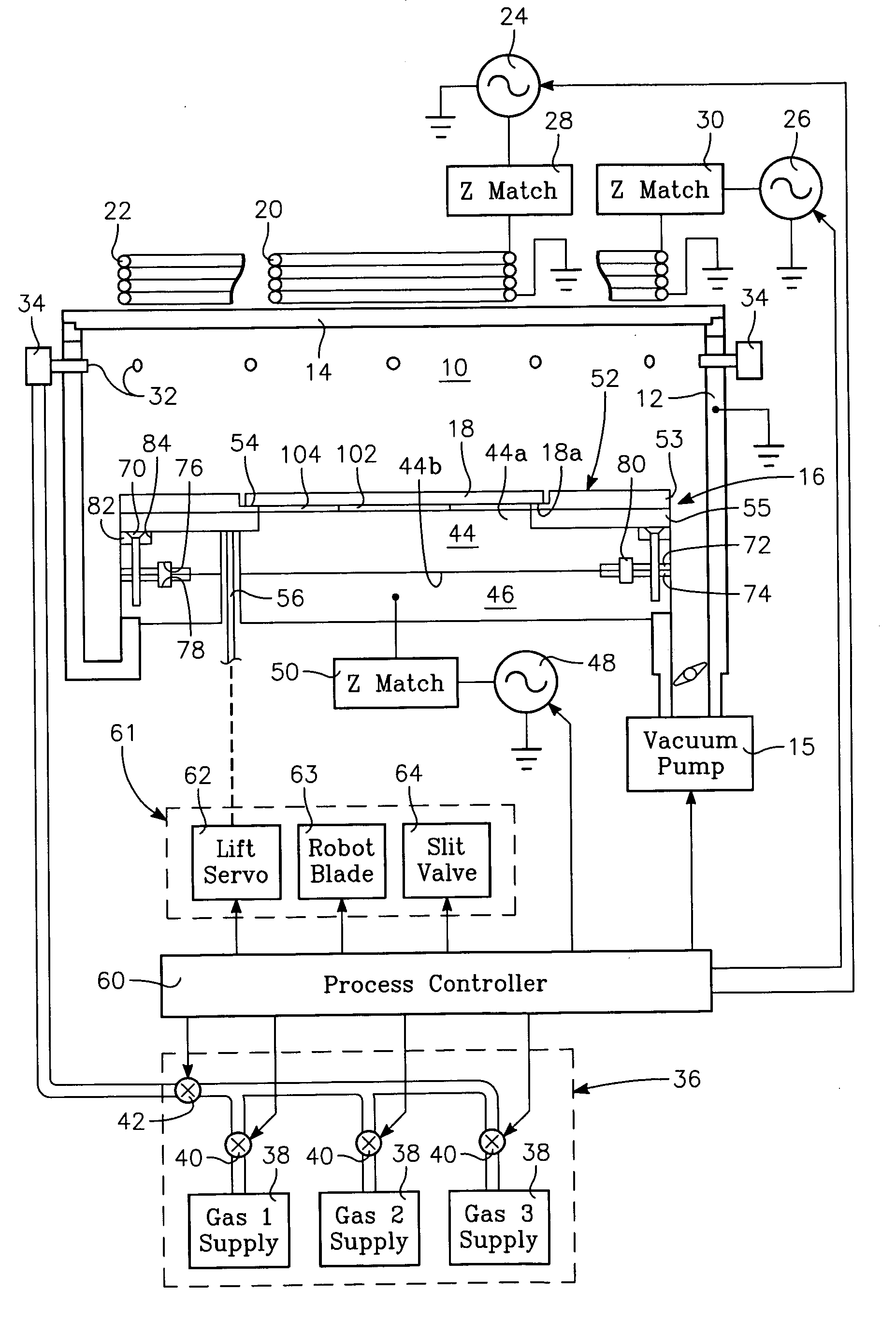
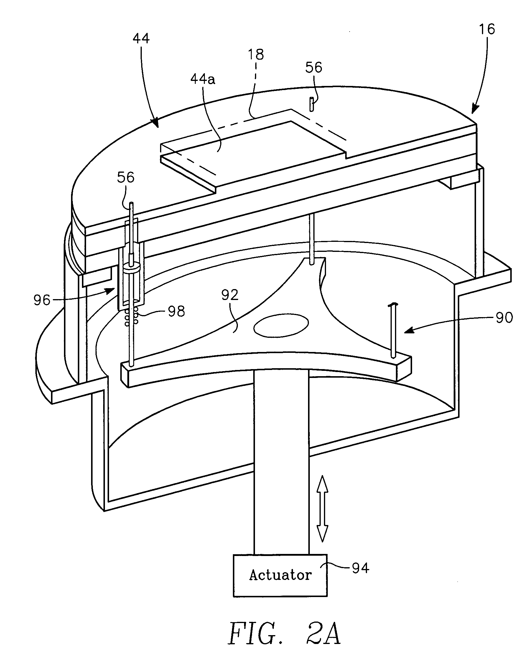
Cathode with Enhanced RF Uniformity:

[0030]We have discovered that one source of non-uniform etch rate distribution in mask etch processes is the existence of RF electrical non-uniformities in the support pedestal or cathode holding the mask in the plasma reactor in which the mask etch process is carried out. RF bias power is applied to the pedestal to control plasma ion energy at the mask surface, while RF source power is applied to an overhead coil antenna, for example, to generate plasma ions. The RF bias power controls the electric field at the mask surface that affects the ion energy. Since the ion energy at the mask surface affects the etch rate, RF electrical non-uniformities in the pedestal create non-uniformities in the distribution of etch rate across the mask surface. We have discovered that there are several sources of RF non-uniformity in the pedestal. One is the titanium screws that fasten the aluminum pedestal (cathode) and aluminum facilities plate together. The screw...


PUM

PropertyMeasurementUnit
Electrical conductivityaaaaaaaaaa
Shapeaaaaaaaaaa
Electrical conductoraaaaaaaaaa

Abstract

A plasma reactor for etching a workpiece such as a rectangular or square mask, includes a vacuum chamber having a ceiling and a sidewall and a workpiece support pedestal within the chamber including a cathode having a surface for supporting a workpiece, the surface comprising plural respective zones, the respective zones of the surface being formed of respective materials of different electrical characteristics. The zones can be arranged concentrically relative to an axis of symmetry of the wafer support pedestal.

Description

BACKGROUND[0001]Fabrication of photolithographic masks for use in processing of ultra large scale integrated (ULSI) semiconductor wafers requires a much higher degree of etch uniformity than semiconductor wafer processing. A single mask pattern generally occupies a four inch square area on a quartz mask. The image of the mask pattern is focused down to the area of a single die (a one inch square) on the wafer and is then stepped across the wafer, forming a single image for each die. Prior to etching the mask pattern into the quartz mask, the mask pattern is written in photoresist by a scanning electron beam, a time consuming process which makes the cost of the mask very high. The mask etch process is not uniform across the surface of the mask. Moreover, the e-beam written photoresist pattern is itself non-uniform, and exhibits, in the case of 45 nm feature sizes on the wafer, as much as 2-3 nm variation in critical dimension (e.g., line width) across the entire mask. (This variation...

Claims


Application Information

Patent Timeline
IPC IPC(8): H01L21/3065
CPCH01J37/3255H01L21/67069H01L21/68785H01L21/68742H01L21/68757H01L21/67253H01L21/3065
Inventor LEWINGTON, RICHARDGRIMBERGEN, MICHAEL N.NGUYEN, KHIEM K.BIVENS, DARINCHANDRACHOOD, MADHAVI R.KUMAR, AJAY
Owner APPLIED MATERIALS INC
Why Eureka
Try Eureka