Electronic Device and Method for Manufacturing Thereof

a manufacturing process and electronic device technology, applied in the direction of semiconductor devices, microstructured systems, semiconductor/solid-state device details, etc., can solve the problems of increasing material costs, increasing manufacturing costs, and difficult to enhance structural integrity between mems structures, so as to reduce the cost of manufacture and minimize the electronic device

Inactive Publication Date: 2008-05-08
SEIKO EPSON CORP
View PDF4 Cites 97 Cited by
  • Summary
  • Abstract
  • Description
  • Claims
  • Application Information

AI Technical Summary

Benefits of technology

[0011]Embodiments of the invention solve the problems described above by highly integrating the functional structure, being disposed in the cavity on the substrate, with an electronic circuit, thereby realizing a more miniaturiz

Problems solved by technology

However, one of the problems of the first method described above, in which two substrates are joined, is that it increases the material cost because it requires another substrate to be used exclusively for the sealing.
In addition, even though the use of an ordinary semiconductor manufacturing technique is desired, the special process of joining the two substrates, which the method requires, diminishes the merit of using the semiconductor manufacturing technique, increasing the manufacturing cost.
Normally, it is difficult to en

Method used


Image

  • Electronic Device and Method for Manufacturing Thereof
  • Electronic Device and Method for Manufacturing Thereof
  • Electronic Device and Method for Manufacturing Thereof

Examples


first embodiment

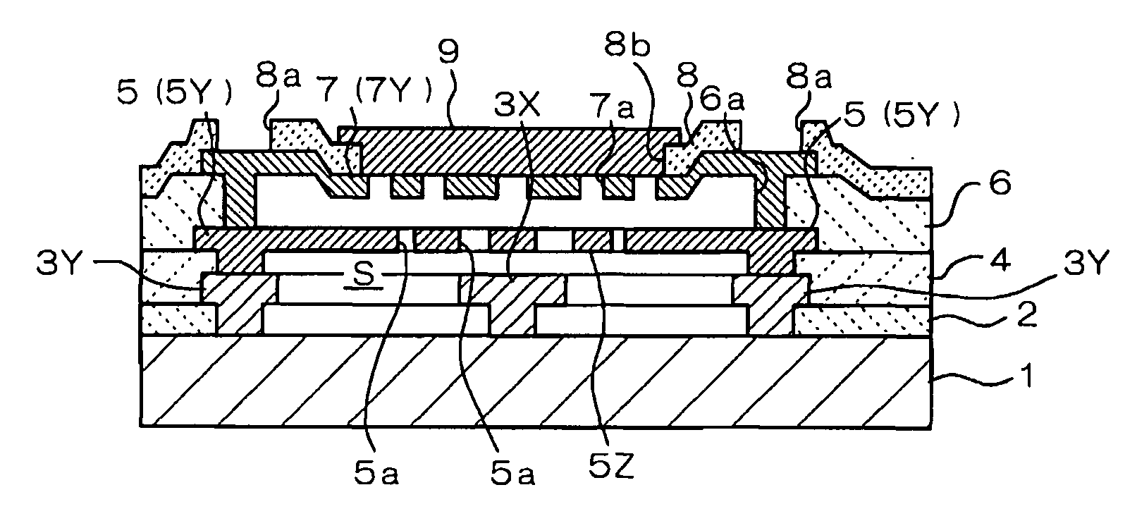
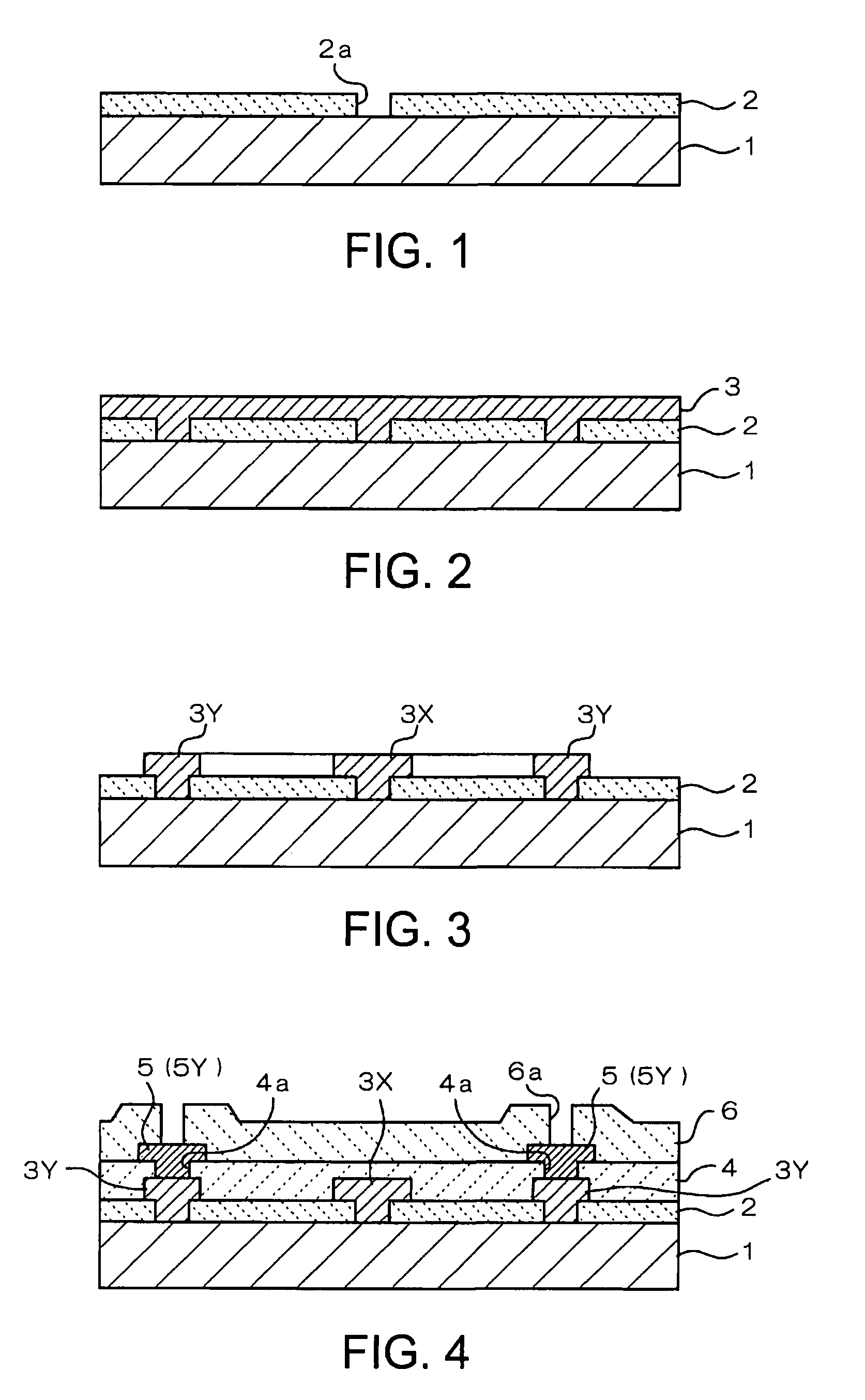
[0036]Referring to FIGS. 1 through 8, a method for manufacturing an electronic device according to one embodiment will be described.

[0037]First, as shown in FIG. 1, a substrate 1 comprised of, e.g., a semiconductor substrate is placed. It is preferable that the substrate 1 is a semiconductor substrate, such as a silicon substrate, but various other substrates including a ceramics substrate, a glass substrate, a sapphire substrate, a diamond substrate, a synthetic resin substrate, and the like, can be used. When a semiconductor substrate is used, a predetermined semiconductor integrated circuit (not illustrated; a metal oxide semiconductor (MOS) transistor, for example) may be fabricated on the substrate 1 either in advance or at some adequate point of the process. The substrate 1 that is used in the manufacturing method according to the present embodiment includes a proper impurity region (not illustrated) on its surface part. Furthermore, the manufacturing method is programmed in s...

second embodiment

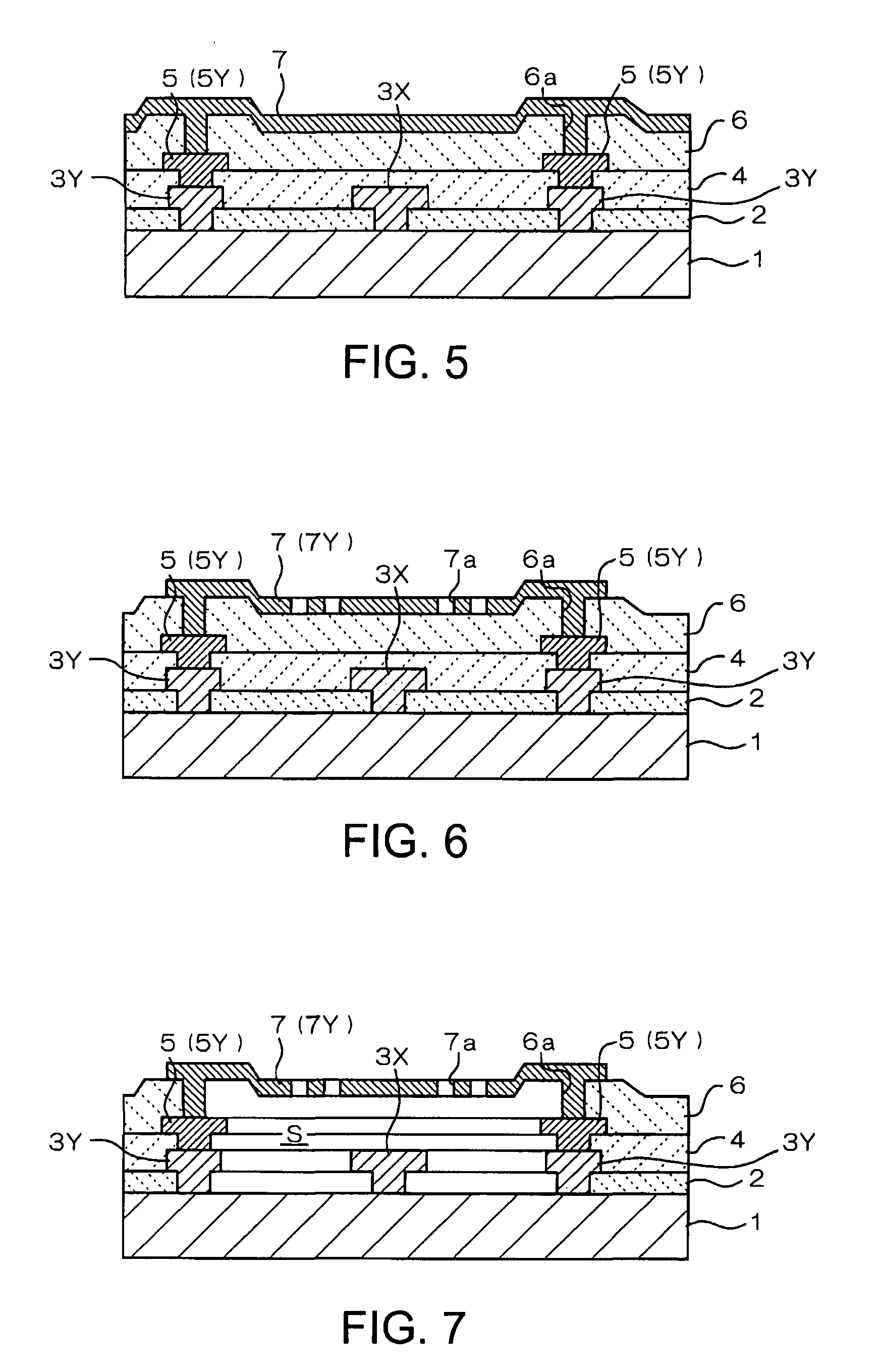
[0055]Referring to FIG. 9, an electronic device according to another embodiment of the will be described. As shown in this illustration, it is preferable that the through holes 7a provided in the first cover layer 7Y are formed in such a manner that they are large enough to allow etching in the release process and small enough to be easily closed by the second cover layer 9. For example, it is preferable that their size is about 1 to 10 μm, more specifically 3 to 5 μm, when reduced to the diameter of an equivalent circle. Also preferable is that the through holes 7a are circular or regularly polygonal in shape (square in the illustrated example) due to the same reasons as above.

[0056]Preferably, the through holes 7a are formed at locations that are somewhat offset from the location right above the MEMS structure 3X. In the illustrated example, the through holes 7a are arranged in such a manner that they exist at locations that are horizontally away from the MEMS structure 3X by as m...

third embodiment

[0061]FIG. 11 illustrates an example in which the above protection film 8 is used as a second cover layer. In this case, it is preferable that the second cover layer 8 is made of an insulating material. The protection film used also as the second cover layer reduces the number of processes (with the above-described deposition and patterning of the second cover layer 9 becoming unnecessary), thereby further lowering the cost of manufacture.


PUM


Abstract

An electronic device, including a substrate, a functional structure constituting a functional element formed on the substrate, and a cover structure forming a cavity portion in which the functional structure is disposed, is disclosed. In the electronic device, the cover structure includes a laminated structure of an interlayer insulating film and a wiring layer, the laminated structure being formed on the substrate in such a way that it surrounds the cavity portion, and the cover structure has an upside cover portion covering the cavity portion from above, the upside cover portion being formed with part of the wiring layer that is disposed above the functional structure.

Description

CROSS-REFERENCE TO RELATED APPLICATION[0001]This application claims priority from Japanese Patent Application No. 2006-302478 filed in the Japanese Patent Office on Nov. 8, 2006, the entire disclosure of which is hereby incorporated by reference in its entirety.BACKGROUND[0002]1. Technical Field[0003]Embodiments of the present invention relate to an electronic device and a method for manufacturing thereof, and more particularly to a structure and a manufacturing process of an electronic device having a functional element such as a micro electromechanical system (MEMS) disposed in a cavity portion formed on a substrate.[0004]2. Related Art[0005]Electronic devices that include a functional element such as a MEMS disposed in a cavity portion formed on a substrate, are generally known. For example, a MEMS such as a micro resonator, a micro sensor or a micro actuator is housed in a cavity portion in an operable state because the micro structure needs to be disposed in a state that permit...

Claims


Application Information

Patent Timeline
IPC IPC(8): H01L29/06H01L21/30
CPCB81B2207/015B81B2207/07B81C1/00246H01L21/7682B81C2203/0714B81C2203/0735B81C2203/0136H01L24/05H01L2924/14H01L2924/00
Inventor SATO, AKIRAWATANABE, TORUINABA, SHOGOMORI, TAKESHI
Owner SEIKO EPSON CORP
Why Eureka
Try Eureka