

Laser direct writing type nanometer periodic structure pattern manufacturing equipment
A periodic structure and laser direct writing technology, applied in microlithography exposure equipment, optics, optical components, etc., can solve the problems of accumulating considerable processing errors, low process reliability, and slow processing speed, etc. High height, good feedback effect, miniaturized heating effect
- Summary
- Abstract
- Description
- Claims
- Application Information
AI Technical Summary
Problems solved by technology
Method used
Image

Examples
Embodiment Construction
[0025] In order to understand the technical characteristics and practical effects of the present invention in detail, and to implement them according to the contents of the description, further drawings (such as Figures 1 to 4 Shown) the preferred embodiment shown in detail is as follows:
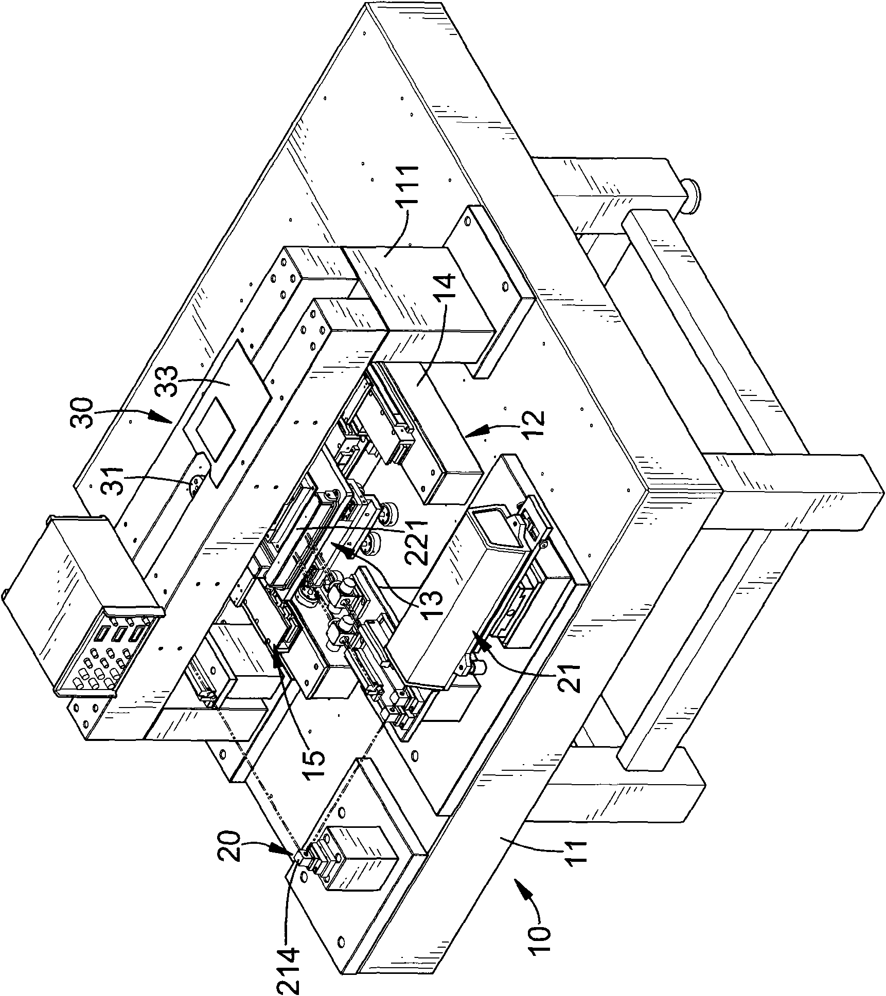
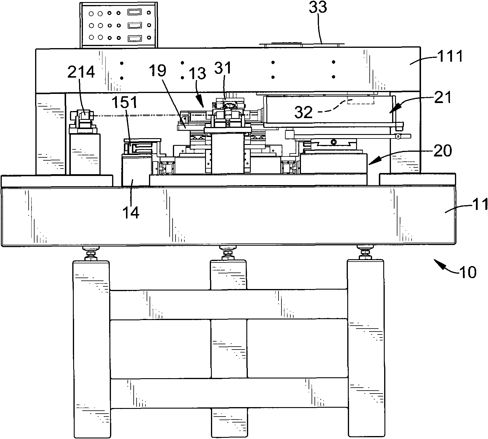
[0026] The present invention provides a laser direct writing nano-periodic structure pattern manufacturing equipment, which includes a platform group 10, a measurement feedback group 20 and a laser direct writing head group 30, wherein:
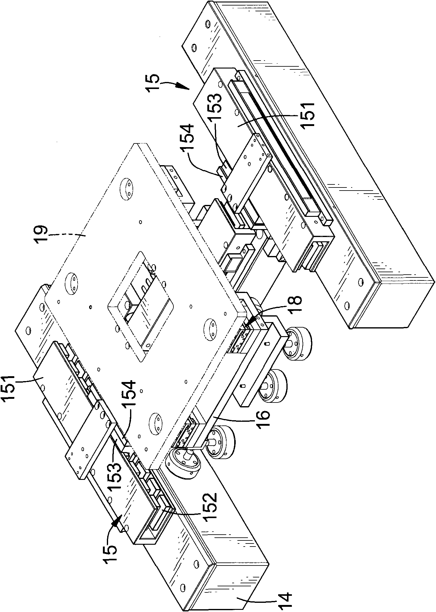
[0027] The platform set 10 is provided with a base 11 and a hybrid mobile platform, wherein the base 11 is provided with a combination frame 111 horizontally on the top surface, and the hybrid mobile platform is provided with a long-stroke mobile platform 12 and a micro-motion piezoelectric platform 13 The long-stroke mobile platform 12 is movably arranged on the top surface of the base 11 and is located below the joint frame 111 and is provided with a re...
PUM
 Abstract
Description
Claims
Application Information