
Method and apparatus for programmably powering down structured application-specific integrated circuits

a technology of integrated circuits and programmable powering, applied in the direction of pulse techniques, instruments, computation using denominational number representation, etc., can solve the problems of low power flow rate, many ales are less than fully utilized, active devices are unusable, etc., to achieve low power targets, eliminate power leakage through unused devices, and high performance design

Inactive Publication Date: 2008-05-08
ALTERA CORP
View PDF16 Cites 0 Cited by
  • Summary
  • Abstract
  • Description
  • Claims
  • Application Information

AI Technical Summary

Benefits of technology

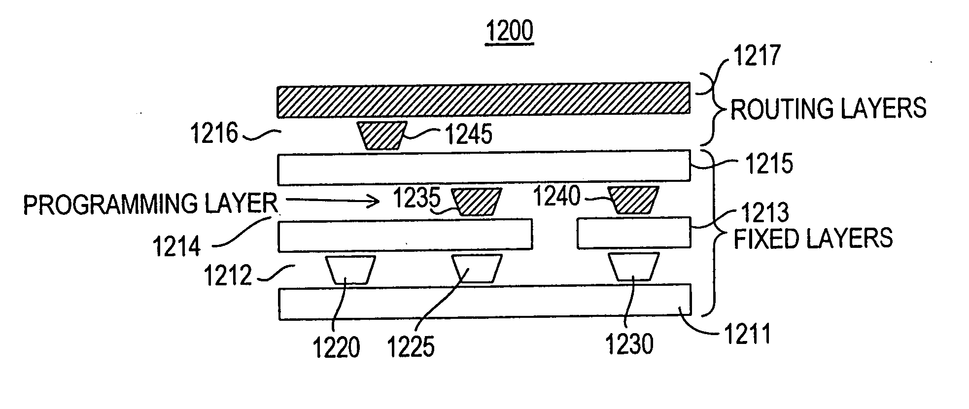
[0010] The present invention relies on at least one of the “programmable” layers of the structured ASIC that frequently provides some programmability as between or among a small number of alternative functions. In accordance with this invention, such a programmable layer is used to configure the power source programming of each logic module of the ASIC design. The layer may be a metallization layer in which programmable connections (e.g., fuses) are used to make or break connections between segments of the layer, or a semiconductor layer in which programmable vias may be used to make or break connections between metallization layers on either side of the semiconductor layer. The present invention eliminates power leakage through unused devices on the structured ASIC, allows for each logic module to be powered down separately, and achieves high performance design while maintaining low power targets in deep sub-micron technology.
[0011] In accordance with one embodiment of the present invention, there is provided a structured application-specific integrated circuit device that includes a plurality of base semiconductor layers and a plurality of base metallization layers, wherein the base layers form at least one hard circuit block at a first location. A first portion of a first one of the metallization base layers at the first location is configured as a first global power bus line for the ASIC device. A second portion of a second one of the metallization base layers at the first location is configured as a first local power bus line for the at least one hard circuit block. A third portion of a third one of the base layers is programmable to control the connection between the first portion of the first one of the metallization base layers and the second portion of the second one of the metallization base layers for programmably powering down the at least one hard circuit block.

Problems solved by technology

This is so because only as many ASIC HLEs as necessary are devoted to performing the functions of each FPGA ALE, and in almost all FPGAs many ALEs are less than fully utilized.
However, in a typical structured ASIC design, some active devices are unusable due to routing or placement constraints.
While this approach may help to reduce the leakage power through the unused device, there is still a small amount of current that will flow through the stable state device as a leakage current.
In deep sub-micron technology, the steady state or off state leakage current becomes higher and introduces a significant impact to the overall power system.

Method used


Image

  • Method and apparatus for programmably powering down structured application-specific integrated circuits
  • Method and apparatus for programmably powering down structured application-specific integrated circuits
  • Method and apparatus for programmably powering down structured application-specific integrated circuits

Examples


Embodiment Construction

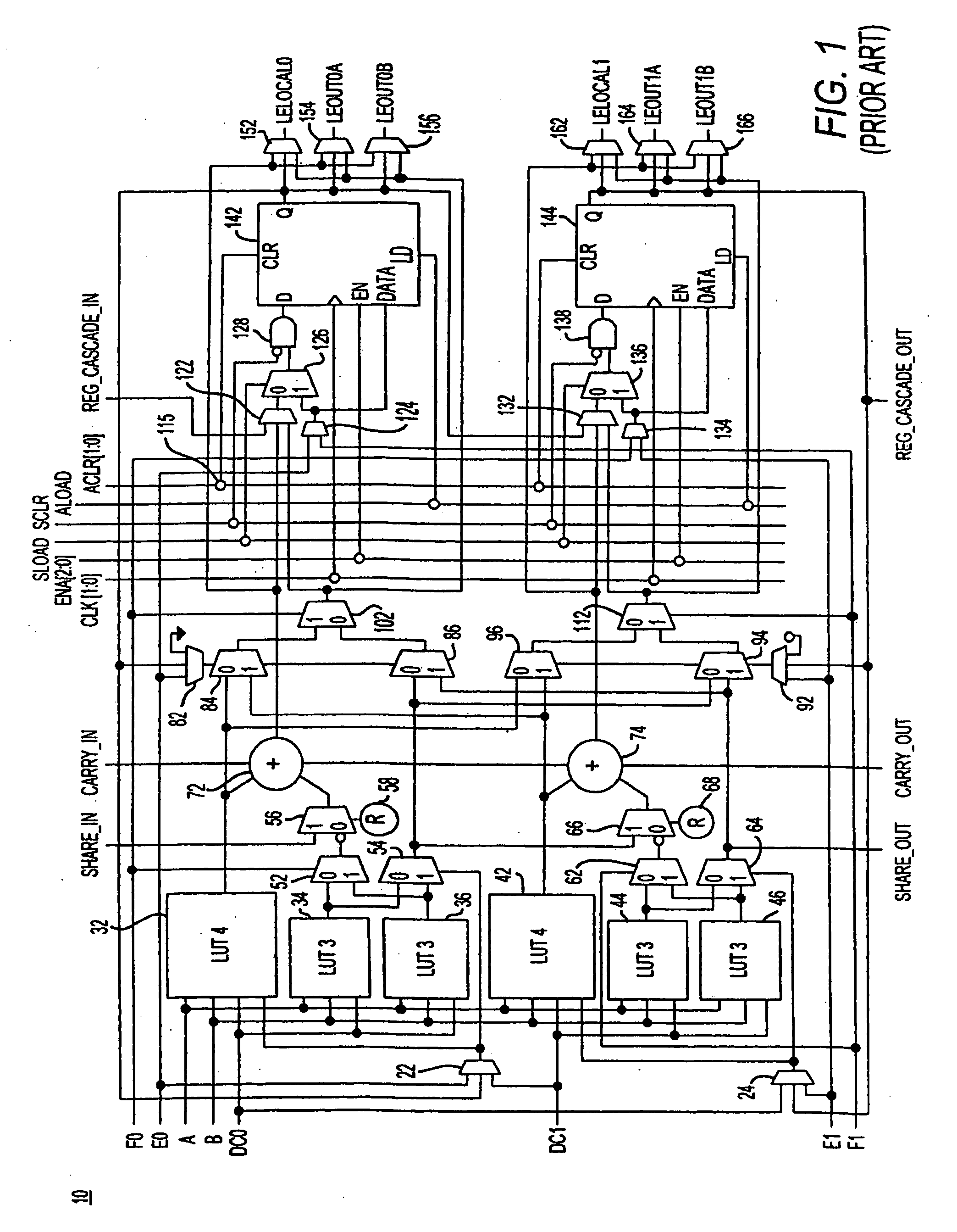
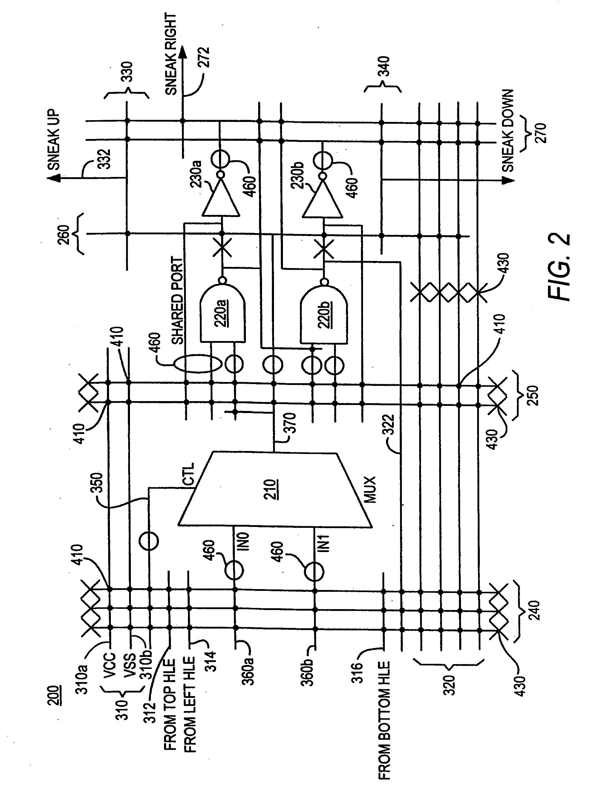
[0023] This specification illustrates the invention in the context of migrating logic designs from a particular type of FPGA to a particular type of structured ASIC. These types of FPGAs and structured ASICs are explained in more detail in such references as Chua et al. U.S. patent application Ser. No. 10 / 884,460, filed Jul. 2, 2004, and Schleicher et al. U.S. patent application Ser. No. 11 / 050,607, filed Feb. 3, 2005, which are hereby incorporated by reference herein in their entireties. To facilitate understanding of the present invention without the need for reference to any other document, however, the next several paragraphs and related FIGS. 1-9 are reproduced (with only minor modifications) from the above-mentioned Chua et al. and Schleicher et al. references.

[0024] An illustrative example of a basic logic circuit building block or unit 10 for inclusion in an FPGA is shown in FIG. 1. This FPGA building block circuitry (also sometimes referred to as an adaptive logic element ...


PUM


Abstract

Methods and apparatus for programmably powering down a structured application-specific integrated circuit are provided. At least one of the programmable layers of the structured ASIC that frequently provides some programmability as between or among a small number of alternative functions is used to provide this programmability.

Description

CROSS REFERENCE TO RELATED APPLICATION [0001] This application is a continuation of U.S. patent application Ser. No. 11 / 119,312, filed Apr. 29, 2005, which is hereby incorporated by reference herein in its entirety.BACKGROUND OF THE INVENTION [0002] The present invention relates generally to structured application-specific integrated circuits (“ASICs”), and more particularly to methods and apparatus for programmably powering down such structured ASICs. [0003] So-called structured ASICs are sometimes used as alternatives to programmable logic devices (“PLDs”), such as field-programmable gate arrays (“FPGAs”). An FPGA has a generic structure that may include many identical blocks of logic circuitry, many registers, and a number of other types of circuit blocks, such as I / O blocks, RAM blocks, DSP blocks, PLL / DLL blocks, etc. These various circuitries are programmable to perform any of a variety of tasks. An FPGA also has a generic interconnection structure. This structure is programma...

Claims


Application Information

Patent Timeline
Patent Type & Authority Applications(United States)
IPC IPC(8): H03K19/177
CPCH03K19/1735
Inventor PHOON, HEE KONGCHUA, KAR KENG
Owner ALTERA CORP
Learn More