
Optical head, exposure apparatus and image forming apparatus

Inactive Publication Date: 2008-05-08
SEIKO EPSON CORP
View PDF2 Cites 4 Cited by
  • Summary
  • Abstract
  • Description
  • Claims
  • Application Information

AI Technical Summary

Benefits of technology

[0008]An advantage of some aspects of the invention is to provide an optical head, an exposure apparatus and an image forming apparatus, which are capable of restricting noise.
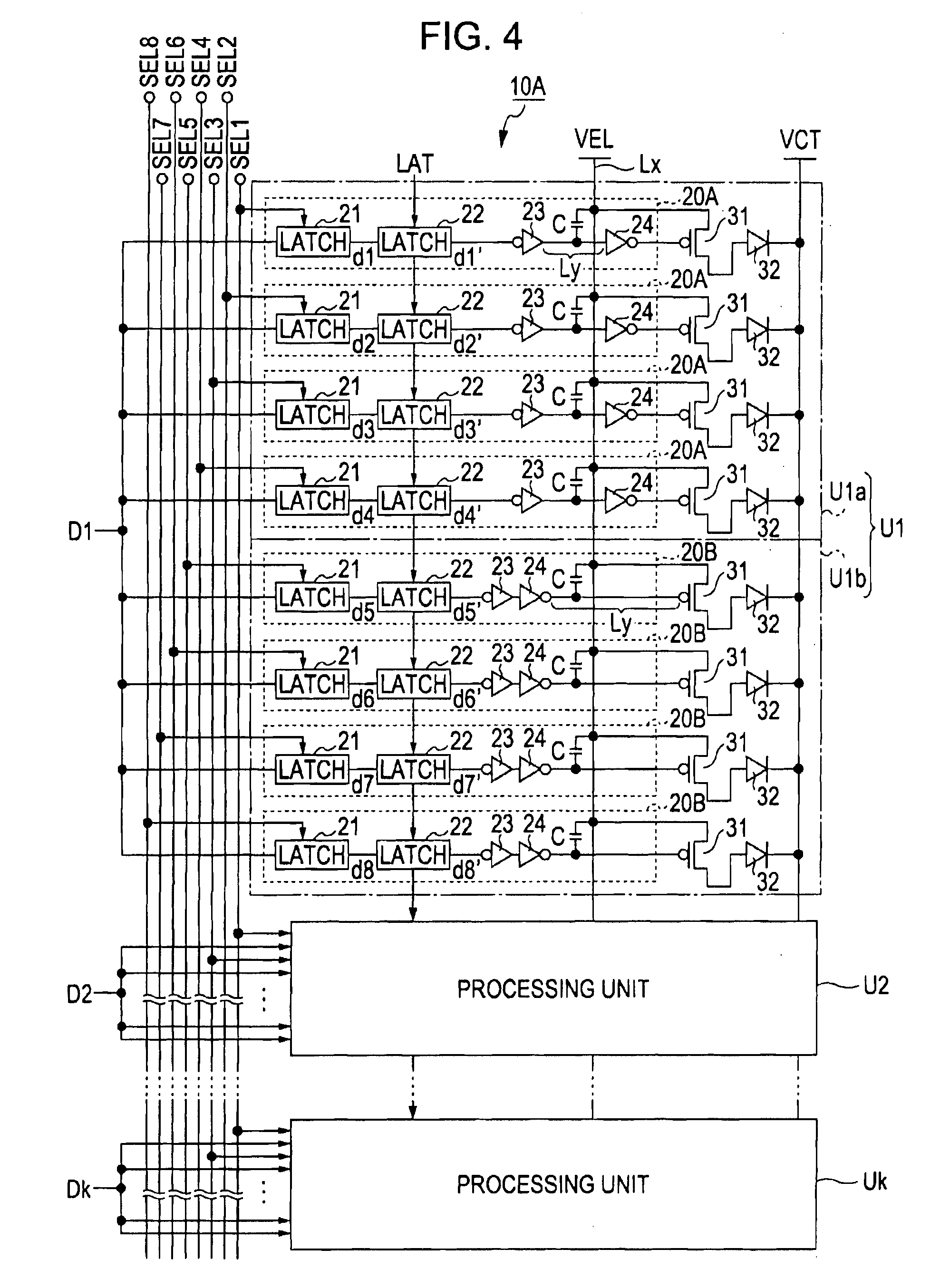
[0010]Parasitic capacitance is produced at the intersection of the line and the potential line. Since the parasitic capacitance acts as coupling capacitance, when the logic level of the line is shifted, noise is superimposed on the potential line. The invention employs an area ratio gray-scale method for representing gray scales. In this case, a pattern of logic levels of the line has blocks as basic units. In addition, since the logic circuits of the plurality of driving circuits invert the logic levels of the lines at the intersection every n natural number of intersections extending in the first direction corresponding to the block, noises superimposed on the potential line can cancel each other out. As a result, print unevenness can be reduced, thereby significantly improving print quality.
[0012]According to another aspect of the invention, there is provided an exposure apparatus including: an optical head according to the first aspect; and a control circuit that generates image data representing gray scales of an image by expressing gray scales of pixels belonging to the block with binary values, and outputs the generated image data to the optical head. With the second aspect of the invention, it is possible to suppress noise and reduce print unevenness.
[0014]According to still another aspect of the invention, since the control circuit generates the image data such that the logic circuits invert logic levels of the lines at the intersections every n natural number of intersections extending in the first direction corresponding to the block, it is possible to suppress noises superimposed on the potential line and reduce print unevenness.
[0016]In this case, since the control circuits invert the image data, the second inverting circuit in the second driving circuit of the optical head may be omitted. As a result, it is possible to simplify the optical head, thereby making it possible to make the optical head smaller.

Problems solved by technology

This produces parasitic capacitance at intersections of the signal lines and the power lines.
Even a minute change in luminance may have an effect on the formation of an electrostatic latent image on a photoconductive drum, which may cause a user to recognize unevenness on a print sheet.
This problem becomes serious in a so-called “solid coating” print.
This is because several pixel circuits make the same logic shift simultaneously, and accordingly, larger noise is added to a power line in the solid coating print.
In this case, although 8000 pixels are divided into blocks, several hundred pixel circuits have to operate simultaneously, which may result in a very high level of noise.

Method used


Image

  • Optical head, exposure apparatus and image forming apparatus
  • Optical head, exposure apparatus and image forming apparatus
  • Optical head, exposure apparatus and image forming apparatus

Examples


first embodiment

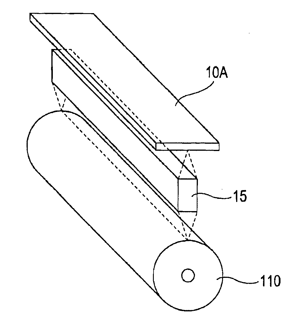
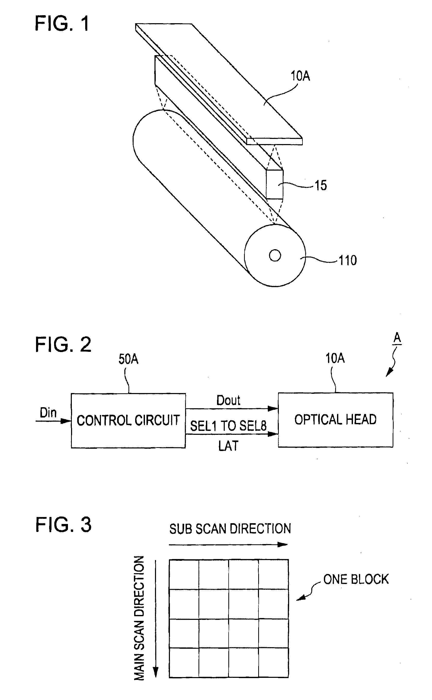
[0037]FIG. 1 is a perspective view showing a configuration of a portion of an image forming apparatus using an optical head according to a first embodiment of the invention. As shown in FIG. 1, the image forming apparatus includes an optical head 10A, a condensing lens array 15 and a photoconductive drum (image carrier) 110. The optical head 10A includes a plurality of light emitting devices arranged in the form of an array. These light emitting devices emit light selectively depending on an image to be printed on a recording material such as a paper. A light emitting device may be any device as long as it can form an electrostatic latent image on the photoconductive drum 110. In the embodiment, for example, an OLED (organic light emitting diode) device may be used as the light emitting device. The condensing lens array 15 is interposed between the optical head 10A and the photoconductive drum 110. The condensing lens array 15 includes a plurality of gradient index lenses arranged i...

second embodiment

[0050]FIG. 10 is a block diagram showing an exposure apparatus B according to a second embodiment of the invention. In the above-described first embodiment, the configuration to invert the logic levels of the lines Ly by the block is completed within the optical head 10A. On the other hand, the exposure apparatus B according to the second embodiment generates output image data Dout′ whose logic levels are inverted in the unit of block in a control circuit 50B. More specifically, as shown in FIG. 11, among d1, d2, d3, d4, . . . , d8 that constitute i-th image data (1≦i≦k) in the output image data Dout of the first embodiment, the control circuit 50B inverts d5 to dB to generate the output image data Dout′. d1 to d4 that constitute image data Di′ are supplied to a block unit Uia corresponding to (2i-1)-th block, and d5a to d8a that constitute the image data Di′ are supplied to a block unit Uib corresponding to 2i-th block. Since d1 to d4 and d5a to d8a are data in the unit of block, t...


PUM


Abstract

An optical head represents gray scales of an image by expressing gray scales of pixels, which belong to a block, with binary values, the block being constituted by n pixels (n is a natural number of 2 or more) in a first direction and m pixels (m is a natural number) in a second direction. The optical head includes: a plurality of light emitting devices that extend in the first direction and emit light with luminance in accordance with driving current; a plurality of driving transistors that are provided corresponding to the plurality of light emitting devices and that supply the driving current; a potential line that applies source potential or gate potential to the plurality of driving transistors; and a plurality of driving circuits that are provided corresponding to the plurality of driving transistors and that supply a driving control signal to specify an ON state or an OFF state for gates of the driving transistors. The driving circuits each include: a line having an intersection at which the line intersects the potential line; and a logic circuit that generates the driving control signal based on image data to instruct turning-on or turning-off of the light emitting devices. The logic circuits of the plurality of driving circuits invert logic levels of the lines at the intersections every n natural number of intersections extending in the first direction corresponding to the block.

Description

BACKGROUND[0001]1. Technical Field[0002]The present invention relates to an optical head driven by an area ratio gray-scale method, an exposure apparatus, and an image forming apparatus using the exposure apparatus.[0003]2. Related Art[0004]An image forming apparatus such as a printer includes an optical head used to form an electrostatic latent image on an image carrier such as a photoconductive drum. The optical head includes a plurality of light emitting devices arranged in the form of an array in a main scanning direction. Light emitting diodes may be used as the light emitting devices.[0005]An example of a method of representing gradation is an area ratio gray-scale method (for example, see JP-A-2004-249549). An area ratio gray-scale method represents gray scales in units of blocks by expressing pixels belonging to blocks, each of which is constituted by n pixels in a main scanning direction and m pixels in a sub scanning direction, with binary values.[0006]In the optical head ...

Claims


Application Information

Patent Timeline
IPC IPC(8): G09G3/36B41J2/44B41J2/45B41J2/455H01L33/00H04N1/036
CPCB41J2/52B41J2/45G03G15/02G03G15/04
Inventor FUJIKAWA, SHINSUKE
Owner SEIKO EPSON CORP
Learn More