Thin film transistor and method of fabricating the same

a thin film transistor and film technology, applied in the field of thin film transistors, can solve the problems of disadvantageous characteristic dispersion of tft, non-uniform distribution of crystal grain boundaries between crystal grains, and limited application range of pm-type oled display devices, etc., to achieve constant directivity and minimize characteristic dispersion

Active Publication Date: 2008-05-15
SAMSUNG DISPLAY CO LTD
View PDF1 Cites 2 Cited by
  • Summary
  • Abstract
  • Description
  • Claims
  • Application Information

AI Technical Summary

Benefits of technology

[0012]Aspects of the present invention provide a thin film transistor including a semiconductor layer with crystal grains of a constant directivity to minimize the characteristic dispersion depending on the crystal grain state, and a method of fabricating the same.

Problems solved by technology

However, the application range of PM-type OLED display devices is restricted to low-resolution small-sized display devices owing to problems of resolution, a high driving voltage, and a shortened life span of materials.
Also, since AM-type OLED display devices consume low power, AM-type OLED display devices can be high-resolution large-sized display devices.
However, the laser crystallization method does not allow for the crystal grains of the polycrystalline silicon to have constant directivity, but rather, crystal grain boundaries between the crystal grains are non-uniformly distributed.
Since the crystal grain boundaries affect characteristics such as electron mobility of TFTs using polycrystalline silicon, the characteristic dispersion of the TFT disadvantageously occurs due to the distribution of the non-uniform crystal grain boundaries when the polycrystalline silicon is formed by the laser crystallization method.

Method used


Image

  • Thin film transistor and method of fabricating the same
  • Thin film transistor and method of fabricating the same
  • Thin film transistor and method of fabricating the same

Examples


Embodiment Construction

[0024]Reference will now be made in detail to the present embodiments of the present invention, examples of which are illustrated in the accompanying drawings, wherein like reference numerals refer to the like elements throughout. The embodiments are described below in order to explain the present invention by referring to the figures.

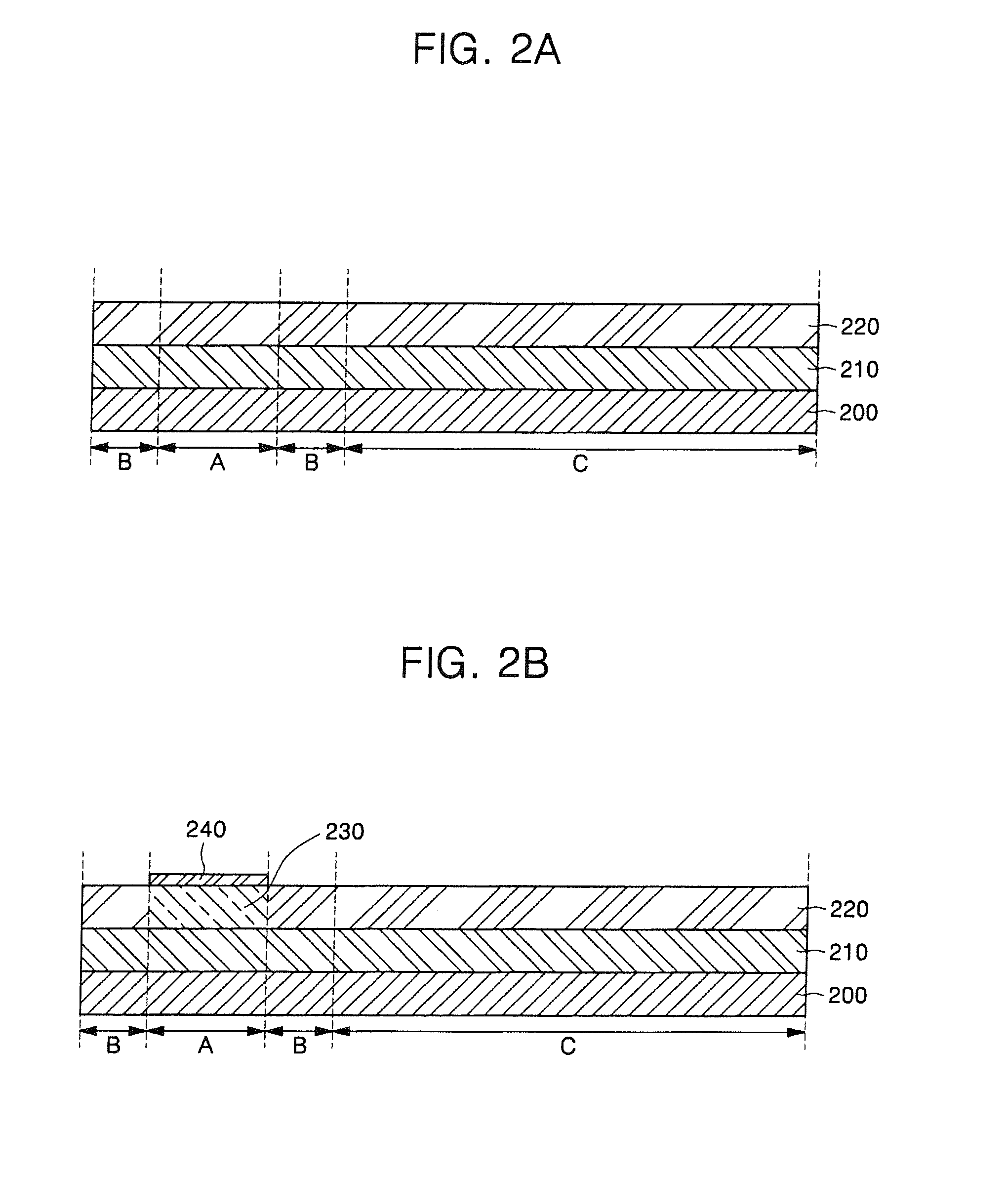
[0025]A TFT according to an embodiment of the present invention includes a semiconductor layer formed of polycrystalline silicon having constant directivity. In order to make the polycrystalline silicon with constant directivity, a P type dopant containing boron is formed in a predetermined region of amorphous silicon, and the doped predetermined region is then used as a seed of the amorphous silicon to be crystallized by a laser crystallization method such as an SLS method or a thin beam directional crystallization (TDX) method.

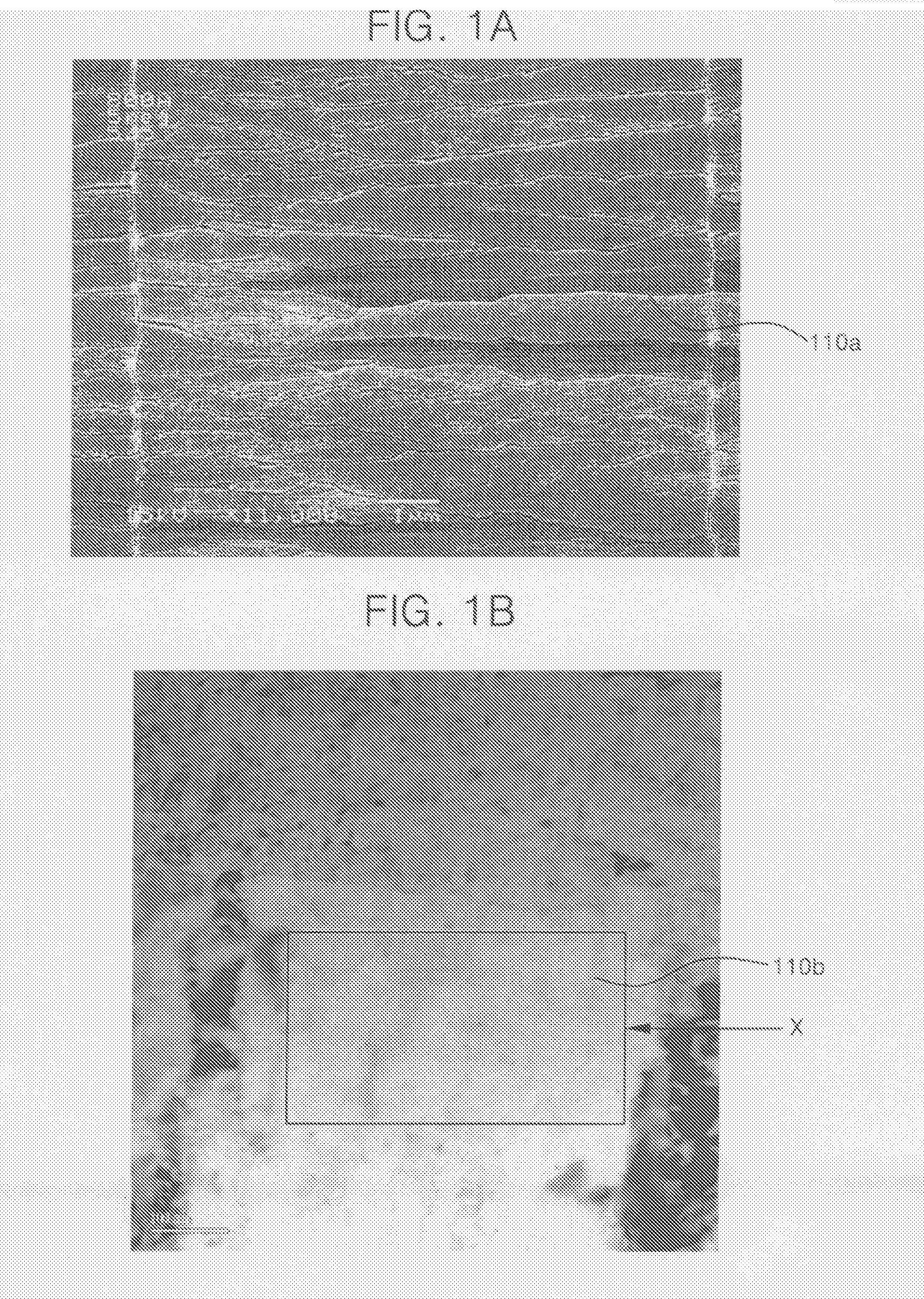
[0026]FIG. 1A illustrates a crystallization state according to a conventional SLS method, and FIG. 1B illustrates a crystalli...


PUM

PropertyMeasurementUnit
temperatureaaaaaaaaaa
crystallization energyaaaaaaaaaa
thicknessaaaaaaaaaa

Abstract

A thin film transistor includes a substrate; a semiconductor layer disposed on the substrate, and including polycrystalline silicon having a constant directivity and a uniformly distributed crystal grain boundary; a gate insulating layer; a gate electrode; an interlayer insulating layer; and source and drain electrodes. The thin film transistor is formed by preparing a substrate including a first region, a second region, and a third region; forming an amorphous silicon layer on the first region, second region, and third region of the substrate; doping a first impurity containing boron into an amorphous silicon layer of the first region; forming a crystallization inducing material on the amorphous silicon layer of the first region; applying crystallization energy to the amorphous silicon layer, and crystallizing the amorphous silicon layers of the first region and the second region adjacent to the first region to form polycrystalline silicon layers; crystallizing the amorphous silicon layer of the third region adjacent to the second region to form a polycrystalline silicon layer using a laser crystallization method; and patterning the polycrystalline silicon layers of the first region, the second region, and the third region to form a semiconductor layer on the third region.

Description

CROSS-REFERENCE TO RELATED APPLICATIONS[0001]This application claims the benefit of Korean Application No. 2006-111189, filed Nov. 10, 2006, in the Korean Intellectual Property Office, the disclosure of which is hereby incorporated herein by reference.BACKGROUND OF THE INVENTION[0002]1. Field of the Invention[0003]Aspects of the present invention relate to a thin film transistor and a method of fabricating the same. More particularly, aspects of the present invention relate to a thin film transistor including a semiconductor layer with crystal grains of constant directivity to minimize the characteristic dispersion depending on the crystal grain state, and a method of fabricating the same.[0004]2. Description of the Related Art[0005]Cathode-ray tubes (CRT) have been superseded by flat panel display devices (FPD) that can be fabricated to be lightweight and thin. Typical examples of FPDs are a liquid crystal display device (LCD) and an organic light emitting diode (OLED) display devi...

Claims


Application Information

Patent Timeline
Patent Type & Authority Applications(United States)
IPC IPC(8): H01L29/04H01L21/336
CPCH01L21/2022H01L27/1277H01L29/78696H01L29/045H01L27/1296H01L21/02672H01L21/02675H01L21/02532
Inventor AHN, JI-SU
Owner SAMSUNG DISPLAY CO LTD
Why Eureka
Try Eureka