Organic light emitting display apparatus employing anode having multi-layer structure

a light-emitting display and multi-layer technology, applied in the direction of discharge tube/lamp details, organic semiconductor devices, discharge tubes luminescnet screens, etc., can solve the problems of increasing manufacturing costs, complicated manufacturing process, and material not suitable for forming an anode for top emission

Inactive Publication Date: 2008-05-15
SAMSUNG MOBILE DISPLAY CO LTD
View PDF10 Cites 58 Cited by
  • Summary
  • Abstract
  • Description
  • Claims
  • Application Information

AI Technical Summary

Benefits of technology

[0009]It is also an object of the present invention to provide a design for an organic light emitting display that is simple to manufacture by reducing eliminating process steps and reducing costs.
[0010]It is further an object of the present invention to provide an organic light emitting display device that has good hole transport properties, high reflectivity, and prevents energy loss due to a drop in voltage.
[0012]The first anode can be made out of a conductive material having a surface resistance less than 0.7Ω / □. The first anode can be made out of a material selected such as Al, AlNd, ACX, AlNiLa, Ag, Mo, Ti and MoW. A thickness of the first anode can be less than 0.5 μm. The second anode can be made out of a conductive material having a work function greater than 6.0 eV. The second anode can be made out of a material such as indium tin oxide and indium zinc oxide. The display device can also include a third anode made out of a conductive material and arranged between the first anode and the planarization layer, the third anode being adapted to prevent contamination of a channel of the semiconductor layer. The first anode can be made out of a material such as Al, AlNd, ACX, AlNiLa and Ag. The third anode can be made out of a material such as Mo, Ti and MoW.

Problems solved by technology

Since a thin film transistor having the above structure is manufactured by separately forming the source and drain electrodes, wires transmitting signals to source and drain electrodes and the pixel electrode, additional mask processes are required, thereby complicating the manufacturing process and increasing manufacturing costs.
Usually, since a material having a high work function has high resistance and low reflectivity, the material is not suitable for forming an anode for top emission.

Method used


Image

  • Organic light emitting display apparatus employing anode having multi-layer structure
  • Organic light emitting display apparatus employing anode having multi-layer structure
  • Organic light emitting display apparatus employing anode having multi-layer structure

Examples


Embodiment Construction

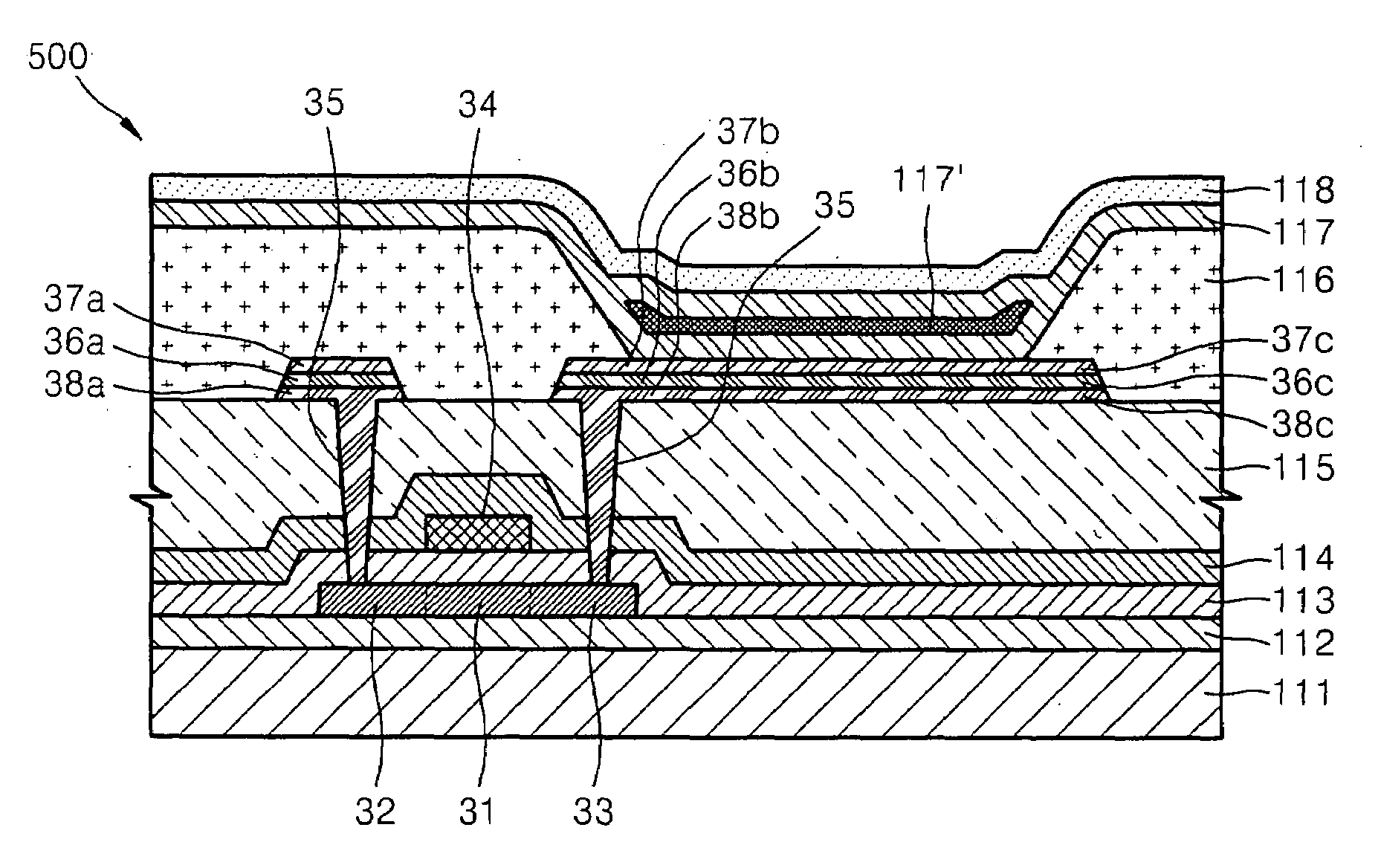
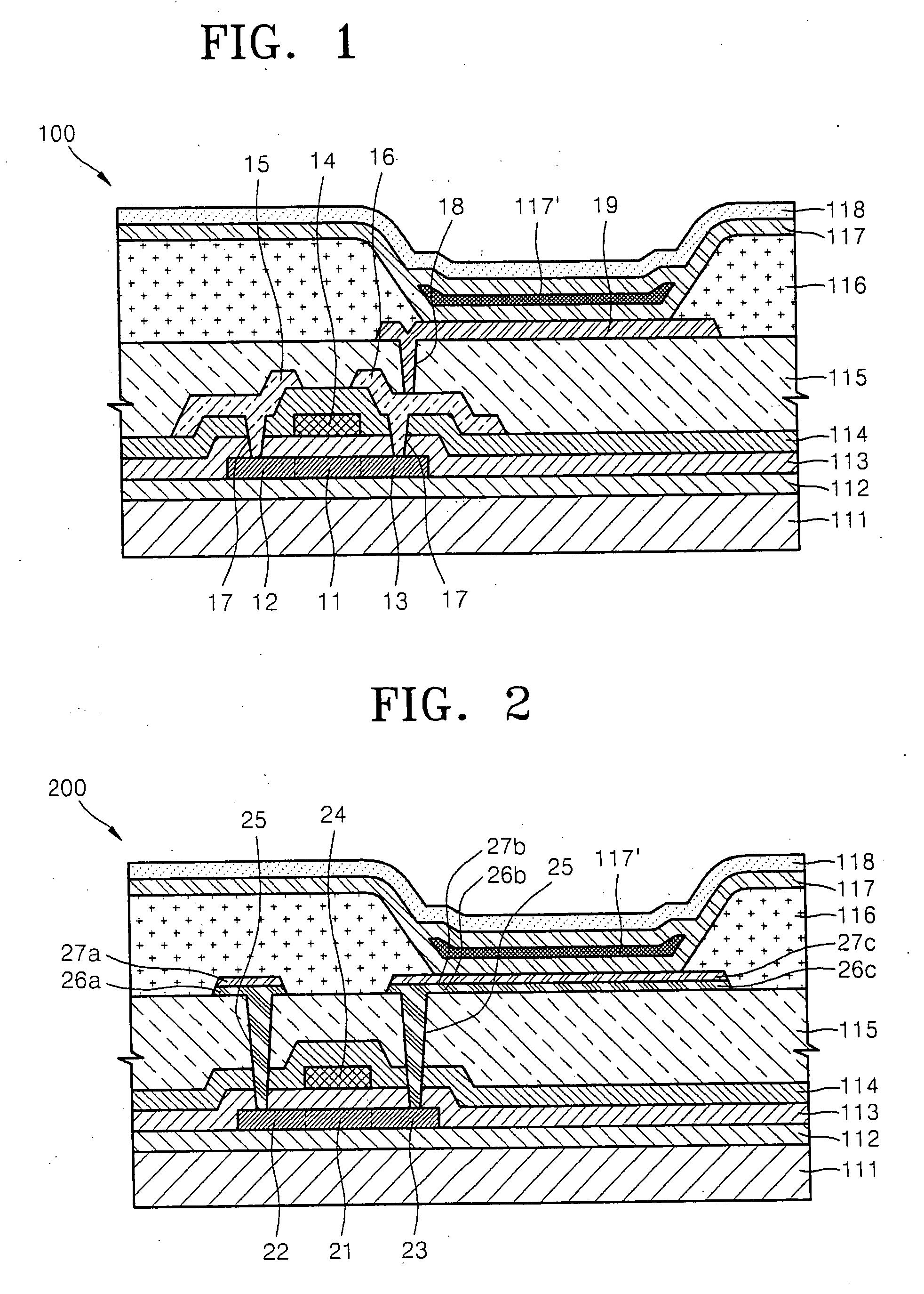
[0024]Turning now to the figures, FIG. 1 is a schematic cross-sectional view illustrating an active matrix (AM) driving type organic light emitting display device 100. Referring to FIG. 1, source and drain electrodes 15 and 16 of the organic light emitting display device 100 are electrically connected to source and drain regions 12 and 13 of a semiconductor layer 11, respectively, through contact holes 17, and are formed on an inter-insulator 114. A planarization layer (and / or passivation layer) 115 is formed on the inter-insulator 114. A pixel electrode formed on the planarization layer 115 is electrically connected to the source or drain electrode 15 or 16 through a via hole 18.

[0025]Since a thin film transistor having the above structure is manufactured by separately forming the source and drain electrodes 15 and 16, wires transmitting signals to source and drain electrodes 15 and 16, and the pixel electrode, additional mask processes are required, thereby complicating the manufa...


PUM


Abstract

An organic light emitting display device including an anode having a multi-layer structure which can be manufactured using a simple process, has good hole transfer properties and high reflectivity, and prevents energy loss due to a drop in voltage. The organic light emitting display device includes a substrate, a thin film transistor formed on the substrate and including source and drain electrodes, a first anode patterned simultaneously with the source and drain electrodes of the thin film transistor, formed integrally with the source or drain electrode, and made out of a conductive material having a low resistance, a second anode formed on the first anode, and made out of a conductive material having a high work function, an organic layer formed on the second anode and a cathode formed on the organic layer.

Description

CLAIM OF PRIORITY[0001]This application makes reference to, incorporates the same herein, and claims all benefits accruing under 35 U.S.C. §119 from an application for ORGANIC LIGHT EMITTING DISPLAY APPARATUS EMPLOYING ANODE HAVING MULTI-LAYER STRUCTURE earlier filed in the Korean Intellectual Property Office on 10 Nov. 2006 and there duly assigned Serial No. 10-2006-0111245.BACKGROUND OF THE INVENTION[0002]1. Field of the Invention[0003]The present invention relates to an organic light emitting display device, and more particularly, to an organic light emitting display device employing an anode having a multi-layer structure that can be manufactured using a simple process, have good hole transport properties and high reflectivity, and prevent energy loss due to a drop in voltage.[0004]2. Description of the Related Art[0005]An organic light emitting display device is a display device including an emission layer made out of an organic material between a pixel electrode and an opposit...

Claims


Application Information

Patent Timeline
Patent Type & Authority Applications(United States)
IPC IPC(8): H01J1/62
CPCH01L27/3248H05B33/26H01L2251/5315H01L51/5218H10K59/123H10K50/818H10K2102/3026
Inventor KWON, DO-HYUNYOO, KYUNG-JINJUN, WOO-SIKKANG, CHUL-KYU
Owner SAMSUNG MOBILE DISPLAY CO LTD
Why Eureka
Try Eureka