Vacuum processing apparatus

Inactive Publication Date: 2008-05-15
HITACHI HIGH-TECH CORP
View PDF9 Cites 19 Cited by
  • Summary
  • Abstract
  • Description
  • Claims
  • Application Information

AI Technical Summary

Benefits of technology

[0019]According to the invention, it is advantageously possible to provide a vacuum processing apparatus and a vacuum proces

Problems solved by technology

Failure to control the wafer orientation eventually deteriorates processing characteristics.
(1) The relative position of the notch of a wafer depends on the shape or arrangement of each processing vessel. Hence, unfortunatel

Method used


Image

  • Vacuum processing apparatus
  • Vacuum processing apparatus
  • Vacuum processing apparatus

Examples


first embodiment

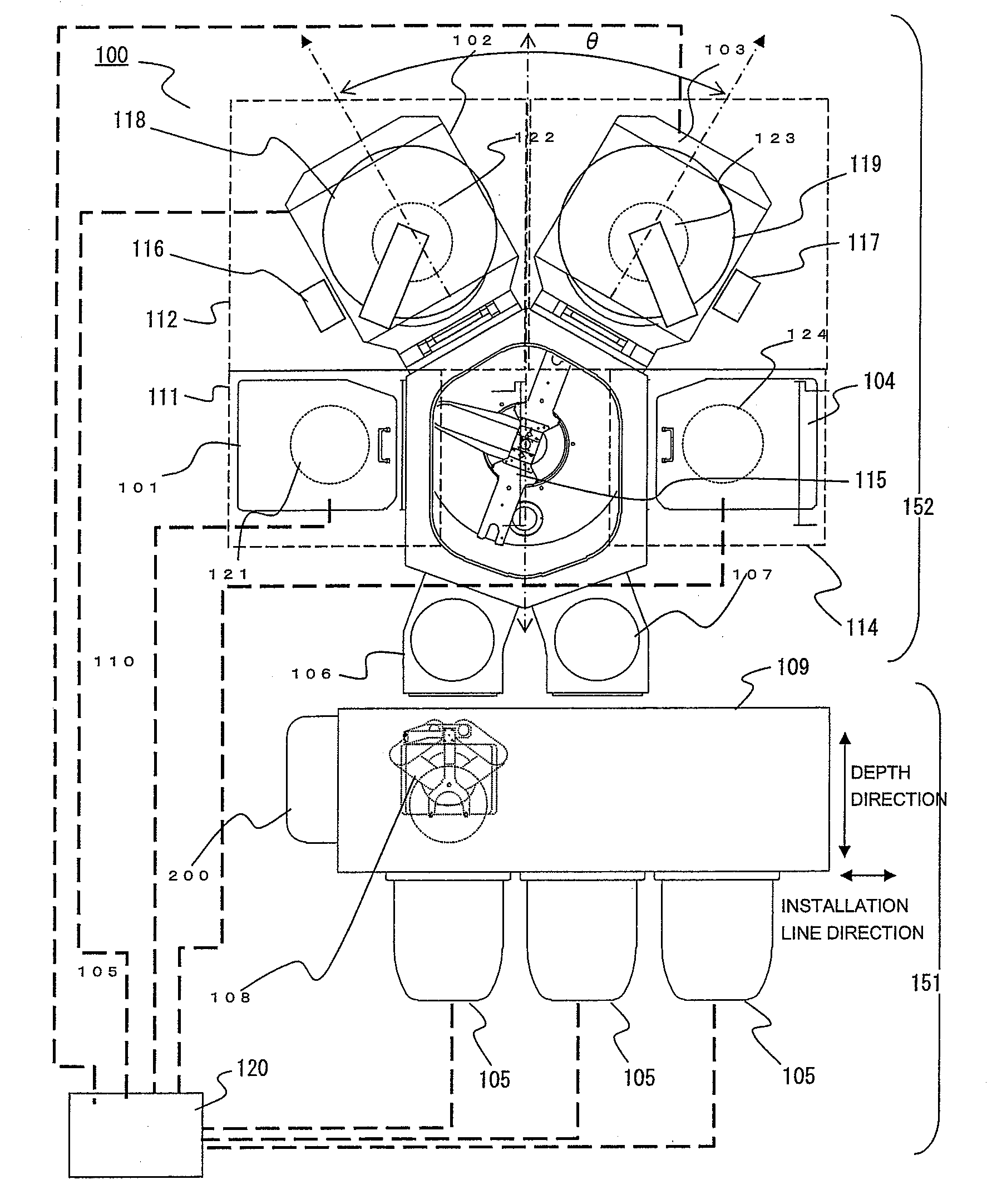
[0029]A first embodiment of the invention is described with reference to FIGS. 1 to 4. FIG. 1 is a top view showing the overall configuration of a vacuum processing apparatus according to the embodiment of the invention. In this figure, the vacuum processing apparatus 100 of this embodiment is divided into two major blocks in the front-to-back direction. The front side section of the vacuum processing apparatus 100, shown on the downside in FIG. 1, is an atmosphere side block 151 where a wafer supplied to the apparatus is transferred to a pressure-reducible chamber under atmospheric pressure and supplied to a processing chamber. On the backside of the vacuum processing apparatus 100, shown on the upside of the atmosphere side block 151 in FIG. 1, is a vacuum side block 152 for processing a subject semiconductor wafer or other substrate sample under vacuum.

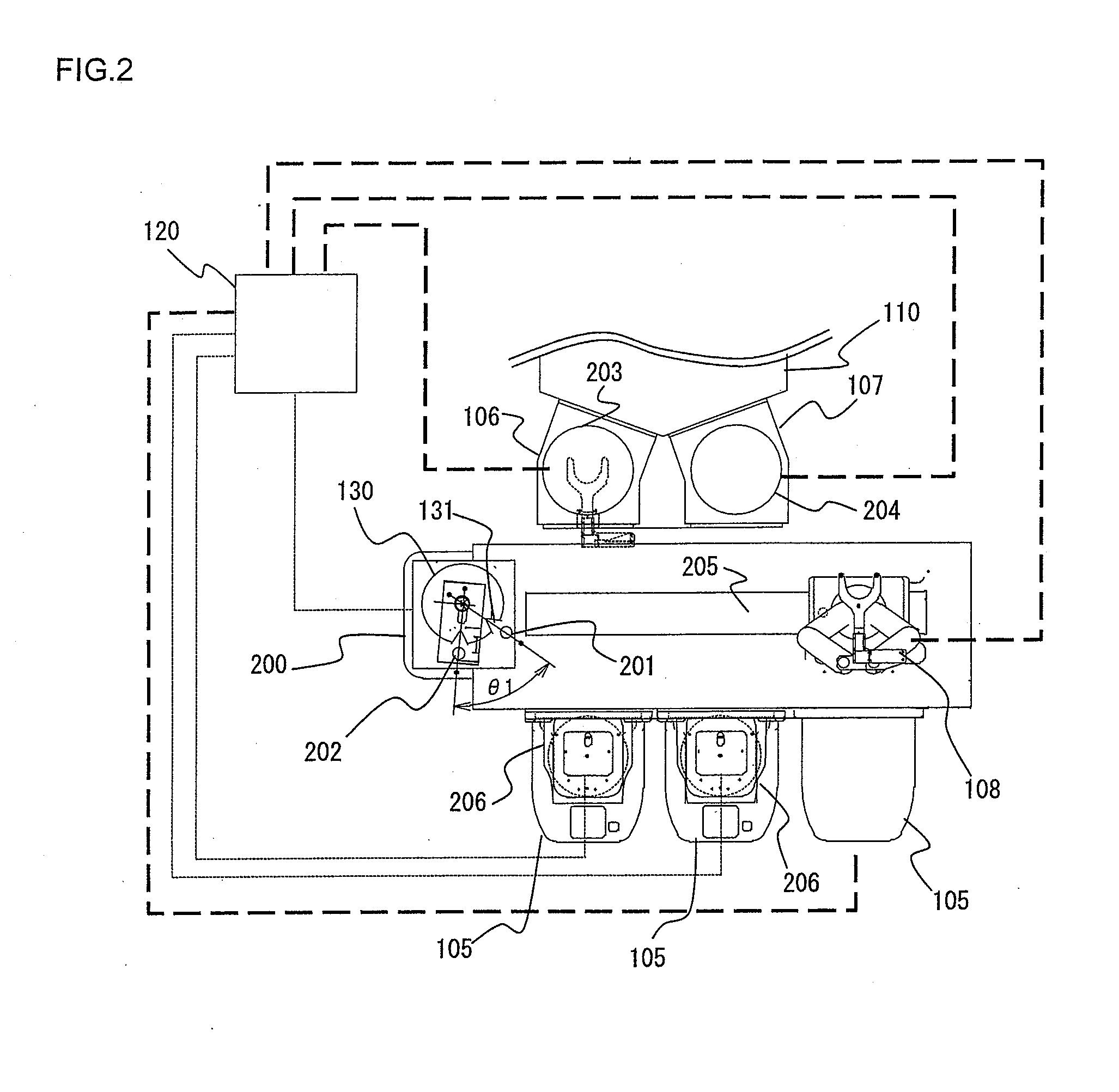
[0030]The atmosphere side block 151 includes a housing 109 equipped therein with an atmospheric transfer robot 108. The atmospher...

second embodiment

[0120]Case 1 of the second embodiment is described with reference to FIGS. 5 and 6. In case 1, there is a structural difference in the vacuum processing apparatus 100. In particular, the processing chambers 101, 102, 103, 104 are different in hardware. For example, FIGS. 5 and 6 illustrate the layout and installation space of the apparatus. The processing units 102, 103 are different in structure due to the symmetrical arrangement. More specifically, the sample stage 122, 123 for mounting a wafer 130 and the waveguide 601, 602 for introducing high-frequency waves for plasma generation are different between the processing unit 102, 103 in the arranging direction, the exhaust direction of process gas and other relative configuration, thereby causing differences in the plasma condition and characteristics in the processing chamber of the processing units 102, 103.

[0121]Thus, if product wafers of exactly the same specification are processed in the processing units 102, 103 of different ...

third embodiment

[0122]Next, case 2 of the third embodiment is described with reference to FIG. 7. In case 2, there are no structural and processing differences in the vacuum processing apparatus 100. That is, the processing units 102, 103 are asymmetrically arranged, and the process characteristics are identical. For example, in the same apparatus, if the process, the material of the subject film, the wafer film specification, and the processing recipe are the same between the processing units 102, 103, and hence the process gas, processing pressure, and applied voltage are the same between the processing units 102, 103, then the plasma condition and characteristics in the processing chamber of the processing units 102, 103 are the same in theory.

[0123]However, in reality, for the following reason, subtle differences often occur in the plasma condition and characteristics. Variations in quality of antennas in the processing chamber, that is, variations of the space due to size differences within th...


PUM


Abstract

The invention provides a vacuum processing apparatus comprising: a plurality of vacuum vessels, each having a processing chamber capable of processing a subject substrate sample placed therein under reduced pressure; a cassette stage for mounting a cassette capable of containing a plurality of the samples; at least one transfer apparatus for transferring the sample from the cassette to the processing chamber in one of the vacuum vessels along a predetermined path and returning the sample processed in the processing chamber to the cassette; and an aligner placed on the path between the cassette stage and the plurality of vacuum vessels for aligning the sample to a predetermined position. The aligner aligns the sample to different positions depending on processings applied to the sample.

Description

[0001]The present application is based on and claims priority of Japanese patent application No. 2006-305139 filed on Nov. 10, 2006, the entire contents of which are hereby incorporated by reference.BACKGROUND OF THE INVENTION[0002]1. Field of the Invention[0003]This invention relates to transferring a semiconductor substrate (hereinafter referred to as “wafer”) between processing chambers of a semiconductor processing system, and more particularly to an apparatus and method for controlling the incision (hereinafter referred to as “notch”) position of a wafer.[0004]2. Description of the Related Art[0005]In a typical vacuum processing apparatus such as a dry etching system, CVD system, or sputtering system, a predetermined number of one or more substrates are treated as a unit (commonly referred to as a lot) and stored in a substrate container, which is then introduced into the system. The processed substrates are also stored in the substrate container and retrieved by the same unit....

Claims


Application Information

Patent Timeline
IPC IPC(8): B65G49/07
CPCH01L21/67167H01L21/68H01L21/67745H01L21/6719
Inventor MATANO, KATSUJIHAMASAKI, RYOJISAKAGUCHI, MASAMICHI
Owner HITACHI HIGH-TECH CORP
Why Eureka
Try Eureka