Printed circuit board and manufacturing method thereof

a technology of printed circuit board and manufacturing method, which is applied in the association of printed circuit non-printed electric components, etching metal masks, and conductive pattern formation. it can solve the problems of complex process, high manufacturing cost, and process for multi-layer printed circuit board. achieve the effect of increasing contact reliability and high density

Inactive Publication Date: 2008-05-22
SAMSUNG ELECTRO MECHANICS CO LTD
View PDF5 Cites 46 Cited by
  • Summary
  • Abstract
  • Description
  • Claims
  • Application Information

AI Technical Summary

Benefits of technology

[0010]An aspect of the invention is to provide a printed circuit board and a method of manufacturing a printed circuit board, with which circuit patterns and lands for forming paste bumps can be formed in a minute scale to form circuit patterns of high density, and in which the paste bumps can be made to cover the lands to increase the contact area between a paste bump and a land and thus increase contact reliability.

Problems solved by technology

However, the conventional manufacturing process for a multi-layer printed circuit board, such as that described above, entails complicated processes and high manufacturing costs, due to the half-etching processes for decreasing the thickness of the copper layer or plating layer and plating processes for filling the BVH's.
Also, forming the circuit patterns by repeatedly plating and etching imposes a limit to implementing high-density circuit patterns, and forming the circuit patterns by a series of stacking layers leads to long processing times.

Method used


Image

  • Printed circuit board and manufacturing method thereof
  • Printed circuit board and manufacturing method thereof
  • Printed circuit board and manufacturing method thereof

Examples


Embodiment Construction

[0023]Embodiments of the invention will be described below in more detail with reference to the accompanying drawings. In the description with reference to the accompanying drawings, those components are rendered the same reference number that are the same or are in correspondence regardless of the figure number, and redundant explanations are omitted.

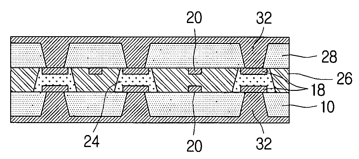
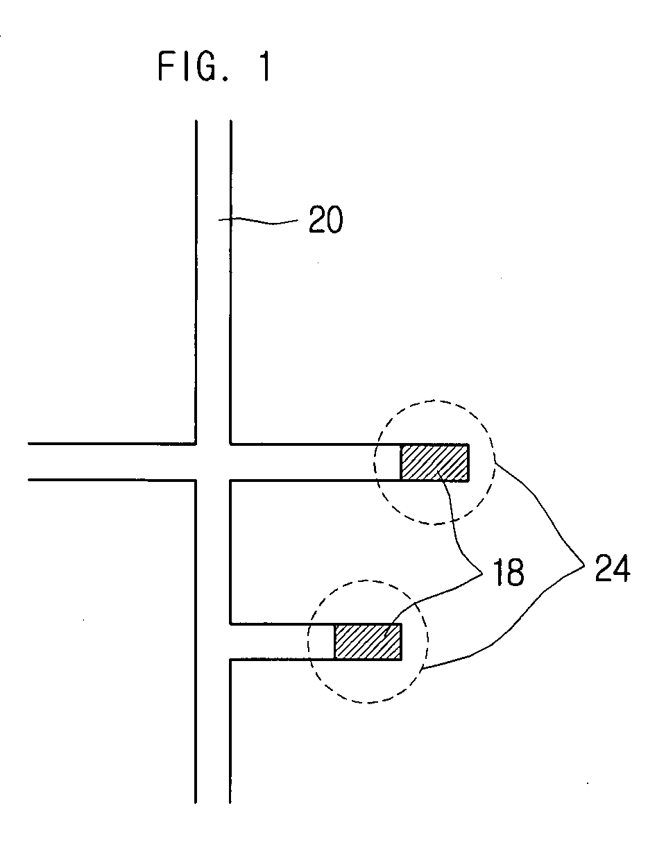
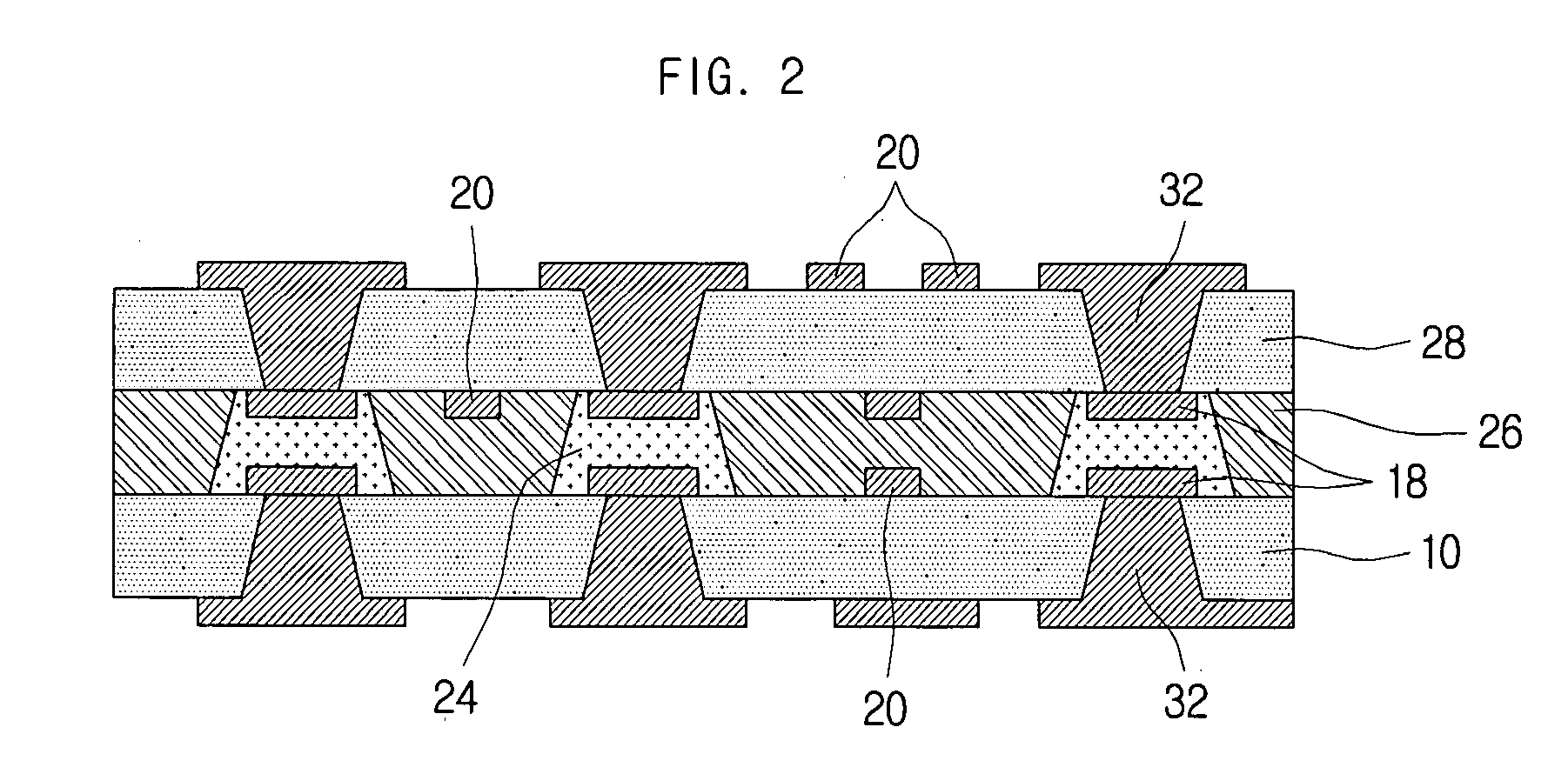
[0024]FIG. 1 is a plan view illustrating paste bumps formed on the lands of a printed circuit board according to an embodiment of the invention, and FIG. 2 is a cross-sectional view illustrating a printed circuit board according to an embodiment of the invention. In FIG. 1 and FIG. 2 are illustrated a first board 10, lands 18, circuit patterns 20, paste bumps 24, a second board 28, an insulation 26, and conductive paste 32.

[0025]A printed circuit board based on this embodiment may be composed of a first board 10, on which a circuit pattern 20 that includes lands 18 is formed, paste bumps 24 formed to cover the lands 18, and an insulati...


PUM

PropertyMeasurementUnit
photosensitiveaaaaaaaaaa
densityaaaaaaaaaa
thicknessaaaaaaaaaa

Abstract

A printed circuit board and a manufacturing method thereof are disclosed. Using a method of manufacturing a printed circuit board which includes forming a circuit pattern, which includes lands, on a first board; forming a paste bump on the land of the first board; and stacking an insulation on a surface of the first board such that the paste bump penetrates the insulation, where the paste bump is formed to cover the land of the first board, the areas of the lands can be reduced to manufacture a printed circuit board of high density, and the contact reliability can be increased due to the increase in contact area between the lands and paste bumps to improve the performance of the high-density printed circuit-board.

Description

CROSS-REFERENCE TO RELATED APPLICATIONS[0001]This application claims the benefit of Korean Patent Application No. 10-2006-0115393 filed with the Korean Intellectual Property Office on Nov. 21, 2006, the disclosure of which is incorporated herein by reference in its entirety.BACKGROUND[0002]1. Technical Field[0003]The present invention relates to a printed circuit board and a method of manufacturing a printed circuit board.[0004]2. Description of the Related Art[0005]The conventional multi-layer printed circuit board is manufactured by forming an inner layer circuit on the surface of a core substrate, such as of a copper clad laminate (CCL), by applying an additive process or subtractive process, and forming outer layer circuits by a method similar to that for the inner layer circuit while sequentially stacking insulation layers and metal layers.[0006]With advances in electronic components, there is a growing demand for technology that can improve the performance of the HDI (high den...

Claims


Application Information

Patent Timeline
Patent Type & Authority Applications(United States)
IPC IPC(8): H05K1/00H05K3/10H05K7/06
CPCH05K3/4069H05K3/462Y10T29/49155H05K2201/09563H05K2203/0554H05K2201/0367H05K3/46
Inventor MOK, JEE-SOOPARK, DONG-JINPARK, JUN-HEYOUNGKIM, KI-HWANKIM, SUNG-YOUNG
Owner SAMSUNG ELECTRO MECHANICS CO LTD
Why Eureka
Try Eureka