Noncontact tag and method for manufacturing the same

a non-contact, tag technology, applied in the direction of burglar alarm mechanical actuation, instrument, hand-held device removal, etc., can solve the problems of fatal damage, unavoidable external stress, and difficult to produce non-contact ic tags cheaply, so as to achieve relatively easy production of non-contact ic tags and avoid external forces

Inactive Publication Date: 2008-05-22
DAI NIPPON PRINTING CO LTD
View PDF4 Cites 21 Cited by
  • Summary
  • Abstract
  • Description
  • Claims
  • Application Information

AI Technical Summary

Benefits of technology

[0032]According to the present invention, since the noncontact IC tag has strip members that are placed in parallel on both sides of the IC chip, the IC chip is positioned in the belt-shaped space between the two strip members and is thus not susceptible to external forces. Therefore, even when this IC tag is handled in a conventional manner, the IC chip in the IC tag is not easily damaged unlike IC chips in conventional IC tags.
[0033]The production method according to the invention is that the step of placing the strip members on both sides of the IC chip is merely added to the conventional production process of a noncontact IC tag. The method of the present invention therefore makes it possible to produce relatively easily a noncontact IC tag having a structure effective for IC chip protection.

Problems solved by technology

However, when noncontact IC tags are used as labels in the field of physical distribution, they are often unavoidably stressed externally.
If the IC chip portions of the noncontact IC tags undergo impacts, their damage is fatal.
However, they are so complicated that they make it difficult to produce noncontact IC tags inexpensively.
It is however not easy to produce such noncontact IC tags.
An unavoidable structural problem with noncontact IC tags is that IC chips are much greater than base films, etc. in thickness.
IC chips are damaged when IC tags are piled up.
If a heavy object is put on top of the pile of the labels, the IC chips impact against one another, and silicon crystals constituting the IC chips are broken.
The noncontact IC tag labels with the IC chips damaged in this manner are regarded as defective even if they are unused.
Another cause of the failure of IC chips is collision of IC tags attached to rigid objects with other rigid objects.
Also in this case, the IC chip portions projecting from the tag surfaces are susceptible to impact.
Although the causes of the failure of IC chips are not limited to the above-described ones, it is considered to be true that thick IC chips tend to be damaged when they are brought into contact with or collide with rigid materials such as metals.
An attempt has been made to flatten not only IC cards but also noncontact IC tags, but it is confronted with a problem that the range of material choice is limited because low prices are desirable for noncontact IC tags.
Further, even if IC tags are made as flat as possible, it is impossible to completely prevent IC chips from being damaged.
The method of making thickness uniform, conventionally adopted in IC cards, is disadvantageous from the viewpoint of reduction in production cost and of material choice.
Further, some difficulties have been found in the actual production process of the noncontact IC tag proposed in the above Patent Document 4.

Method used


Image

  • Noncontact tag and method for manufacturing the same
  • Noncontact tag and method for manufacturing the same
  • Noncontact tag and method for manufacturing the same

Examples


first embodiment

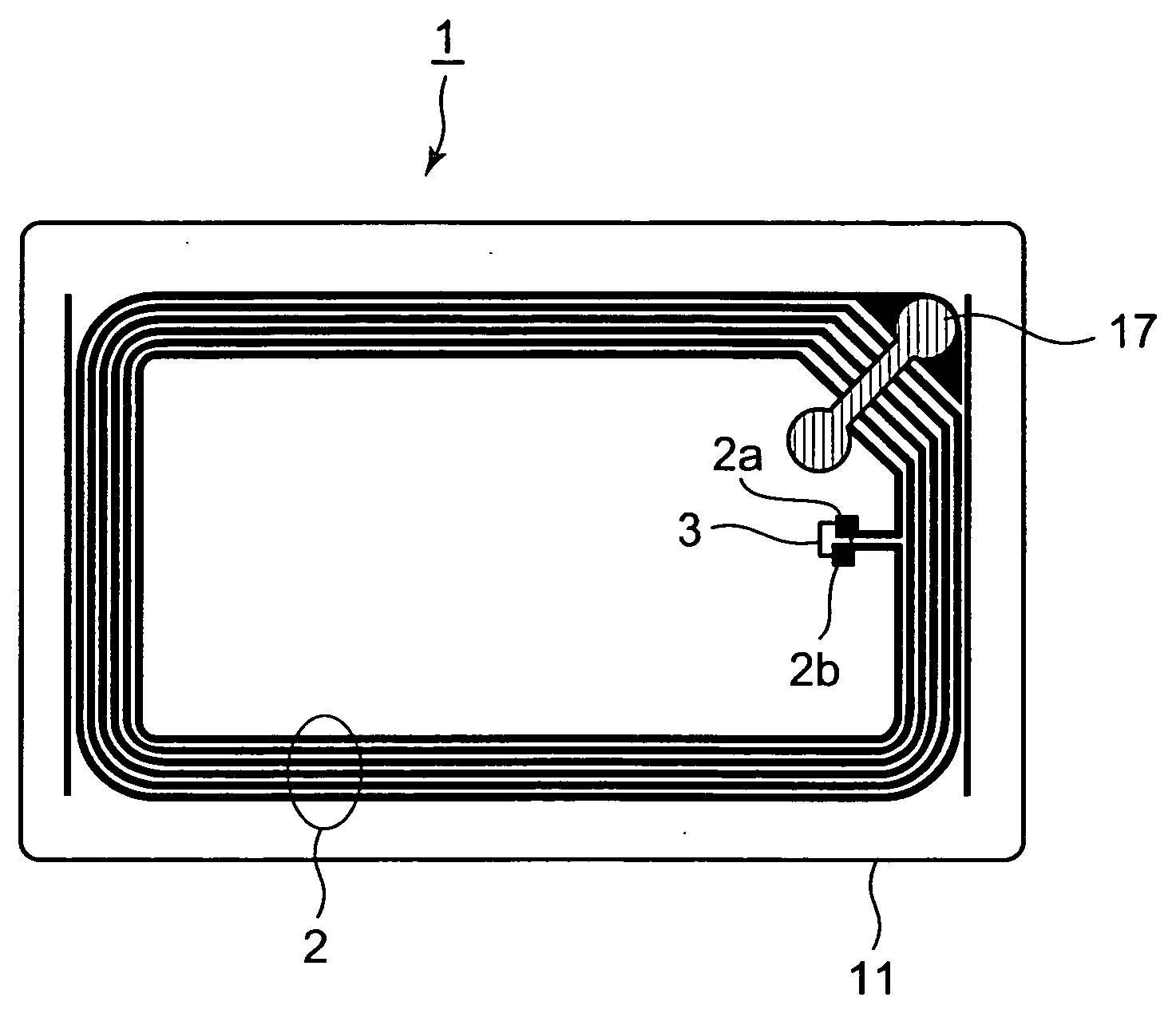
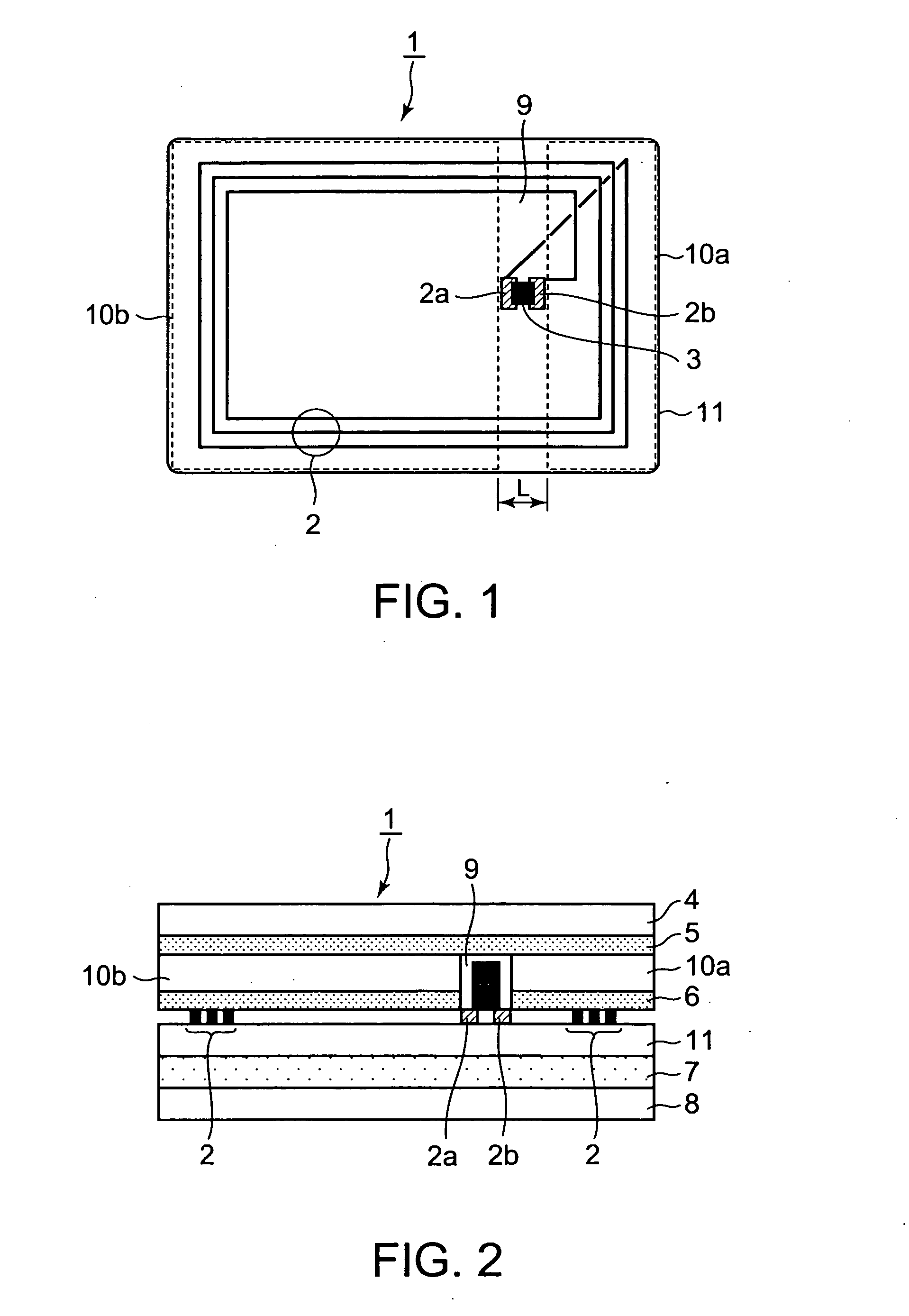
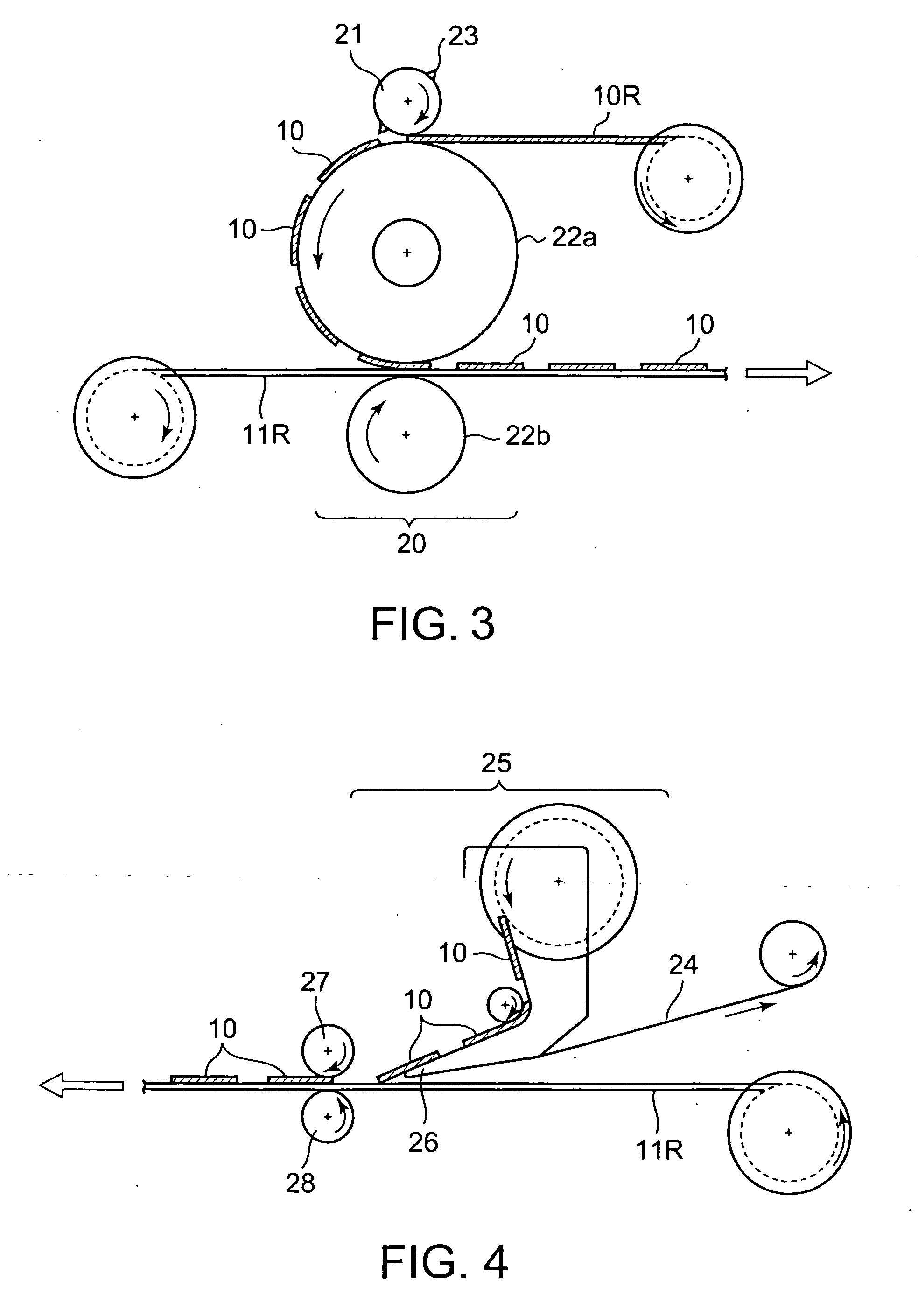
[0046]The present invention relates to a noncontact IC tag having a structure effective for IC chip protection (hereinafter simply referred to as a “noncontact IC tag”) and to a method for producing the noncontact IC tag. With reference to the accompanying drawings, the present invention will be described hereinafter. FIG. 1 is a diagrammatic plan view of a noncontact IC tag of the present invention, and FIG. 2, a sectional view of the noncontact IC tag. FIG. 3 is a view illustrating a method for producing a noncontact IC tag, and FIG. 4 is a view illustrating another method for producing a noncontact IC tag. FIGS. 5(A) and 5(B) are views illustrating a processing method for producing a noncontact IC tag.

[0047]As shown in FIG. 1, a noncontact IC tag 1 of the present invention comprises a base film 11, an antenna pattern 2 formed on the base film 11, and an IC chip 3 connected to both ends 2a, 2b of the antenna pattern 2.

[0048]On both sides of the IC chip 3, two strip members 10a, 10...

second embodiment

[0096]The present invention relates to a flame-retardant tag in the form of a noncontact IC tag, a resonance tag, or a magnetic tag. The flame-retardant tag of each type will be described hereinafter with reference to the accompanying drawings.

[0097]FIG. 7 is a plan view of a flame-retardant tag of the present invention, in the form of a noncontact IC tag, and FIG. 8 is a sectional view of the flame-retardant tag shown in FIG. 7. FIG. 9 is an exploded perspective view of a flame-retardant tag, in the form of a resonance tag, of the present invention. FIG. 10 is an exploded perspective view of a flame-retardant tag, in the form of a magnetic tag, of the present invention, and FIG. 11 is a plan view of a magnetic tag in the form of a label.

[0098]As shown in FIG. 7, a flame-retardant tag 110, in the form of a noncontact IC tag, of the present invention comprises a base film 111, an antenna coil (antenna pattern) 112 formed on the base film 111, and an IC chip 113 connected to both ends...

example 1

[0142]A laminate of a halogen-free, flame-retardant ABS resin (an alloy of ABS and PC (polycarbonate)) sheet with a thickness of 50 μm (“PSZ950” manufactured by Shin-Etsu Polymer Co., Ltd., Japan) and aluminum foil with a thickness of 25 μm, obtained by dry lamination, was used as the base film 111 of a noncontact IC tag label. A photosensitive resist was applied to this base film. The resist surface was covered with a photomask having antenna coil patterns and was then exposed to light. After conducting exposure development, the resist layer was photo-etched, whereby an inlet base film having antenna coils 112 as shown in FIG. 7 was obtained. The external size of each antenna coil 112 was made about 45 mm×76 mm.

[0143]To both ends 112a, 112b of each antenna coil 112 on the above-described inlet base film 111, an IC chip 113 with a plane size of 1.0 millimeter square and a thickness of 150 μm was connected by hot pressing with the IC chip 3 facing down. A 50-μm thick surface-protecti...


PUM


Abstract

A noncontact IC tag 1 comprises a base film 11, an antenna pattern 2 and an IC chip 3 that are on the base film 11, and a surface-protective member 4 covering the antenna pattern 2 and the IC chip 3. Between the surface-protective member 4 and the base film 11 are present two strip members 10a, 10b that are placed in parallel on both sides of the IC chip 3 so that a bet-shaped space 9 is made between them. The IC chip 3 is positioned in this belt-shaped space 9. For the strip members 10a, 10b, it is preferable to use, paper, a plastic film, or a magnetic sheet with a uniform thickness of 50 to 250 μm.

Description

BACKGROUND OF THE INVENTION[0001]1. Field of the Invention[0002]The present invention relates to a noncontact tag and to a method for producing the same. More particularly, the present invention relates to a noncontact tag having an IC chip that is protected from external forces by being positioned in a space between two strip members that are placed in parallel on both sides of the IC chip, and to a method for producing the noncontact tag.[0003]Although the noncontact IC tag of the invention can be used as a conventional tag, it is particularly suitable for use under such circumstances that tags are susceptible to external forces, such as in transportation, physical distribution, and production processes of articles, and at construction sites.[0004]2. Background Art[0005]Noncontact IC tags have come to be used widely as identification media in the fields of transportation, physical distribution, etc., or for such purposes as quality control, stock control, etc. because information ...

Claims


Application Information

Patent Timeline
Patent Type & Authority Applications(United States)
IPC IPC(8): G08B13/14
CPCG06K19/07722G06K19/0773G06K19/07749G08B13/244G08B13/2417G08B13/2437G06K19/07771
Inventor OGATA, TETSUJIIMAIZUMI, KIYOSHI
Owner DAI NIPPON PRINTING CO LTD
Why Eureka
Try Eureka