Plasma etching method and apparatus

a technology of plasma and etching, applied in the direction of electrical equipment, decorative arts, electric discharge tubes, etc., can solve the problem of difficulty in coping with the change of uniformity

Inactive Publication Date: 2008-05-22
SAMSUNG ELECTRONICS CO LTD
View PDF11 Cites 19 Cited by
  • Summary
  • Abstract
  • Description
  • Claims
  • Application Information

AI Technical Summary

Benefits of technology

[0020]The foregoing and / or other aspects and utilities of the present general inventive concept may also be achieved by providing a plasma etching apparatus including upper and lower electrodes facing each other within a chamber, an etching target disposed on the lower electrode and having a multilayer structure, a plurality of upper RF power supplies to apply a first RF power to the upper electrode, a plurality of lower RF power supplies to apply a second RF power to the lower electrode, a switch to individually turn on or off each of the plurality of upper and lower RF power supplies to adjust ion density and ion energy within the chamber, and a controller to control an operation of the switch to sequentially generate specific ion densities and ion energies within the chamber in association with properties of respective layers of the etching target to optimally etch the respective layers.

Problems solved by technology

If the wafer as an etching target has a multilayer structure, each layer may require an ion density and ion energy different from other ion densities and ion energies associated with other layers to obtain optimal etching, causing difficulty in coping with change of uniformity caused by variation of the etching process.

Method used


Image

  • Plasma etching method and apparatus
  • Plasma etching method and apparatus
  • Plasma etching method and apparatus

Examples


Embodiment Construction

[0037]Reference will now be made in detail to the embodiments of the present general inventive concept, examples of which are illustrated in the accompanying drawings, wherein like reference numerals refer to the like elements throughout the drawings. The embodiments are described below to explain the present general inventive concept by referring to the figures.

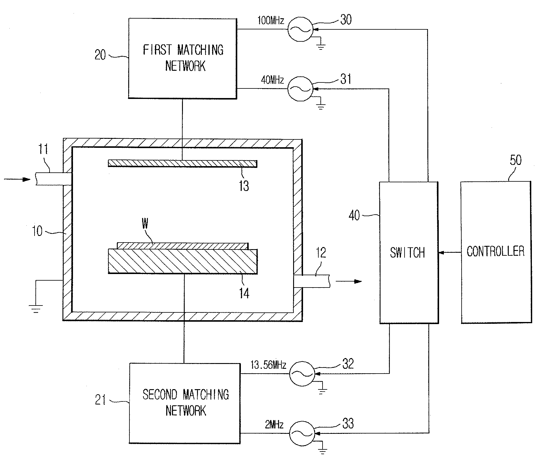
[0038]As illustrated in FIG. 1, the plasma etching apparatus according to an embodiment of the general inventive concept includes a chamber 10 that has a predetermined volume and is formed with a gas inlet 11 and a gas outlet 12. The chamber 10 is grounded. An etching gas is induced into the chamber 10 through the gas inlet 11, and discharged from the chamber 10 to an outside through the gas outlet 12.

[0039]The chamber 10 has an upper electrode 13 and a lower electrode 14 facing each other therein. The upper and lower electrodes 13 and 14 are formed from a conductive material, and have a planar shape. The lower electrode 14 ...


PUM

PropertyMeasurementUnit
frequencyaaaaaaaaaa
frequencyaaaaaaaaaa
ion densityaaaaaaaaaa

Abstract

A plasma etching method and apparatus. In the plasma etching apparatus, pluralities of RF power supplies are respectively connected to upper and lower electrode via relevant matching networks to enable generation of various ion densities and ion energies of plasma by individually changing RF powers applied to the upper and lower electrodes through control of the RF power supplies, so that the plasma etching apparatus can perform all processes which includes a process requiring a low ion density and a low ion energy, a process requiring the low ion density and a high ion energy, a process requiring a high ion density and the low ion energy, and a process requiring the high ion density and the high ion energy, thereby realizing various plasma etching processes.

Description

CROSS-REFERENCE TO RELATED APPLICATIONS[0001]This application claims priority under 35 U.S.A. §119(a) of Korean Patent Application No. 2006-0113959, filed on Nov. 17, 2006, in the Korean Intellectual Property Office, the disclosure of which is incorporated herein in its entirety by reference.BACKGROUND OF THE INVENTION[0002]1. Field of the Invention[0003]The present general inventive concept relates to a plasma etching method and apparatus, and, more particularly, to a plasma etching method and apparatus which can process semiconductor wafers with plasma.[0004]2. Description of the Related Art[0005]Generally, plasma refers to an ionized gas composed of positive ions, negative ions, electrons, excited atoms, molecules, chemically highly active radicals, etc. Since plasma has very different electrical and thermal properties from those of normal gases, it is also referred to as the fourth material state. As plasma includes ionized gas, it is usefully applied to semiconductor manufactur...

Claims


Application Information

Patent Timeline
Patent Type & Authority Applications(United States)
IPC IPC(8): C23F1/00H01L21/302
CPCH01J37/32091H01J37/32183H01J37/32165H01L21/3065
Inventor SUNG, DOUG YONGKWON, TAE YONG
Owner SAMSUNG ELECTRONICS CO LTD
Why Eureka
Try Eureka