Method for manufacturing semiconductor device

a manufacturing method and semiconductor technology, applied in the direction of semiconductor devices, basic electric elements, electrical equipment, etc., can solve the problems of deterioration of the etching speed of the sige layer in some areas, large area differences and density differences, and slowing down speed, so as to improve the process yield and stabilize the electric property , the effect of improving the etching selectivity

Inactive Publication Date: 2008-08-14
138 EAST LCD ADVANCEMENTS LTD
View PDF5 Cites 15 Cited by
  • Summary
  • Abstract
  • Description
  • Claims
  • Application Information

AI Technical Summary

Benefits of technology

[0010]An advantage of the present invention is to provide a method for manufacturing a semiconductor device capable of improving the process yield and stabilizing the electric property.
[0011]The inventors executed various experiments regarding selective etching of SiGe with hydrofluoric-nitric acid. From results of the experiments, the inventors found such selective etching mechanism that SiGe serves as an anode while Si serves as a cathode in the selective etching, and SiGe is removed by an electrochemical reaction such as the one shown in FIG. 18.
[0012]That is, the inventors consider that the “deterioration of the etching selectivity” is caused by decrease of oxidation number of SiGe or increase of oxidation number of Si due to insufficient supply of holes to a SiGe layer when SiGe is selectively etched.
[0013]The inventors also consider that the “roughness of the under surface of the SOI layer and the upper surface of the Si substrate” is caused by the following reason. In a case where the SiGe layer is present in the SiGe selective etching, holes transfer from the Si substrate to the SiGe layer. Thus the oxidation number of the SiGe layer increases, advancing the SiGe etching. On the other hand, since electrons are excessively present (that is, the oxidation number is small) in the Si layer and the Si substrate, Si is not etched. However, after the SiGe layer is removed, holes cannot transfer from Si to SiGe so as to increase the oxidation number of Si. Therefore holes transfer to the etchant as Si++, so that Si is etched. Namely, the under surface of the Si layer and the upper surface of the Si substrate serve as both of the anode and the cathode in a random manner so as to advance the etching of Si. Therefore, the under surface of the Si layer and the upper surface of the Si substrate get rough.
[0014]In particular, in the SiGe selective etching, after HNO3 and HF molecules reach the surface of SiGe, the SiGe layer becomes a H2Si (or Ge)F6 reaction product at the interface between the SiGe layer and the etchant so as to be removed. Here, when Si or Ge is denoted as IV (group), the removal reaction is shown as a formula 1.IV+HNO3+6HF→H2IVF6+HNO2+H2O+H2   (1)
[0015]In this reaction, HNO3 serves as an oxidizer so as to form an oxide IVO2 on the surface of the SiGe layer, while HF works to dissolve the oxide.

Problems solved by technology

However, in a circuit mounting a bulk silicon device together with an SOI device, and in a circuit mounting devices employing different driving voltages, area difference and denseness difference are generally large between plane patterns of the SOI layer.
Here, in a related art manufacturing method, an etching speed of the SiGe layer deteriorates in some areas due to the irregularity of the patterns (that is, the speed slows down).
Especially, if the etching time is lengthened, an accelerated Si etching disadvantageously occurs.
Therefore, it is hard to form an SOI layer with a large area having a stable shape and an even film thickness or an SOI layer in various shapes with high yields.
In the manufacturing method in related art, during the extra etching after the remove of the SiGe layer (that is, over-etching), an under surface of the Si layer (that is, the SOI layer) and an upper surface of the Si substrate facing the cavity get rough, disadvantageously producing irregularities thereon.
If the under surface of the SOI layer and the upper surface of the Si substrate get rough, the evenness of the film thickness of the SOI layer deteriorates.
Therefore, the adhesiveness of the SOI layer with respect to the Si substrate through the thermal oxide films (that is, the BOX layer) disadvantageously deteriorates.
On the other hand, since electrons are excessively present (that is, the oxidation number is small) in the Si layer and the Si substrate, Si is not etched.
However, after the SiGe layer is removed, holes cannot transfer from Si to SiGe so as to increase the oxidation number of Si.
Therefore, the under surface of the Si layer and the upper surface of the Si substrate get rough.

Method used


Image

  • Method for manufacturing semiconductor device
  • Method for manufacturing semiconductor device
  • Method for manufacturing semiconductor device

Examples


first embodiment

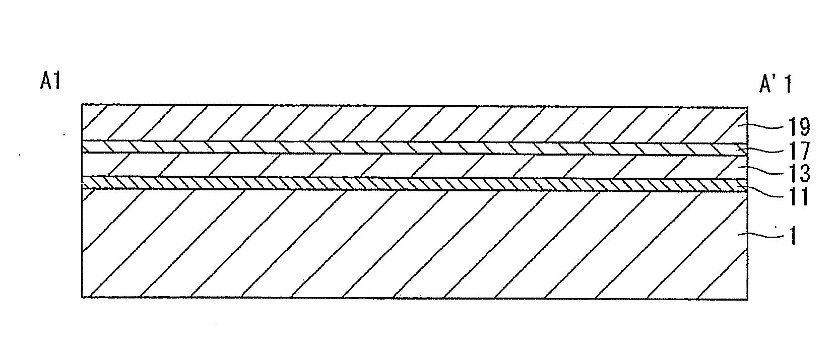
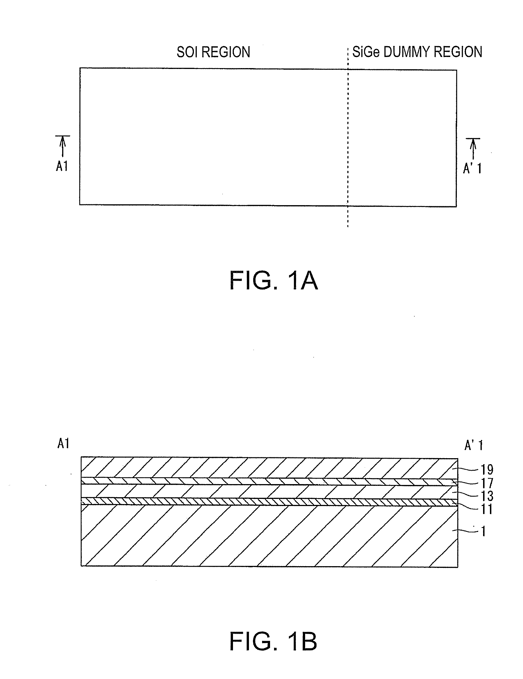
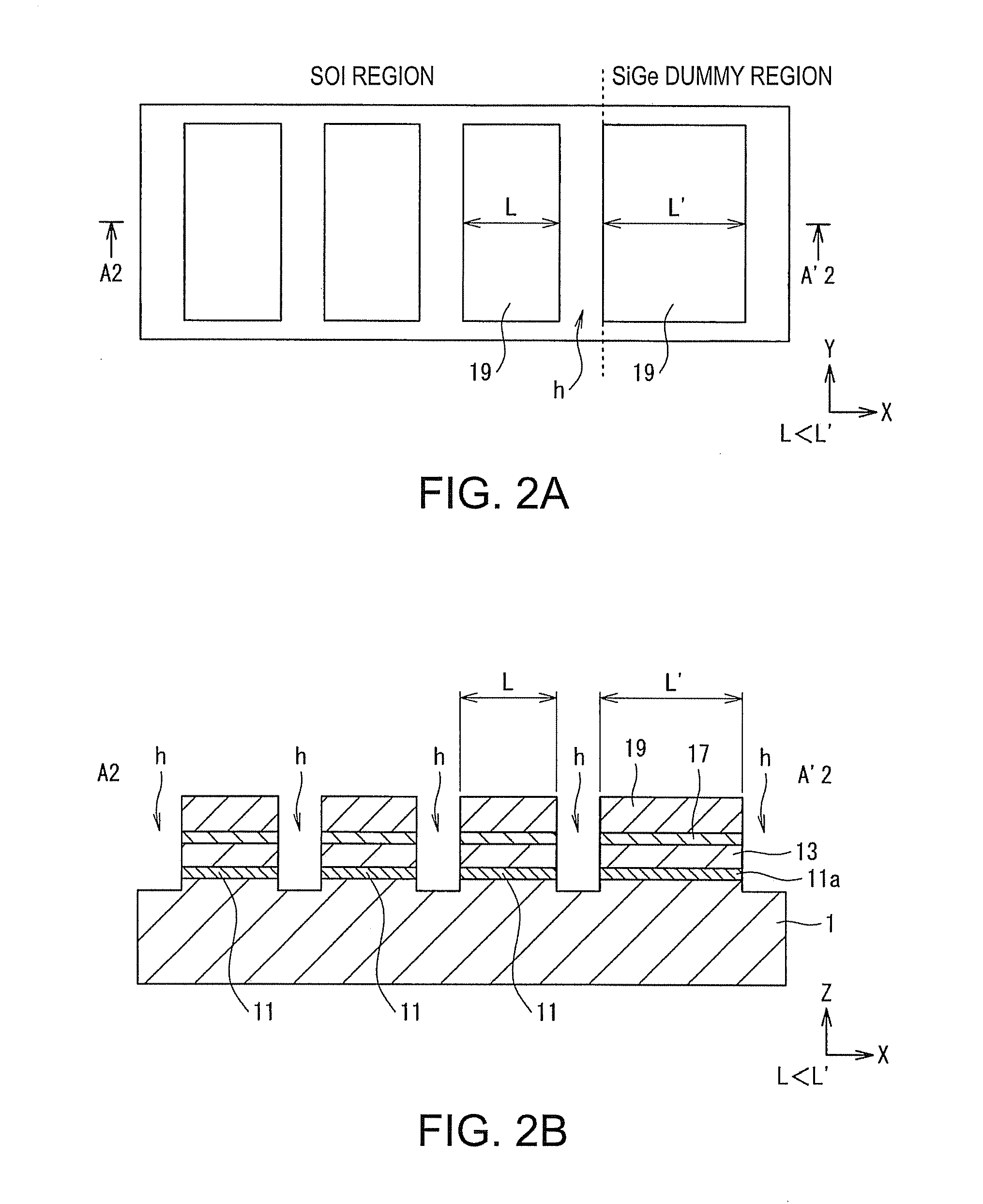
[0060]FIGS. 1A through 8B are diagrams showing a method for manufacturing a semiconductor device according to a first embodiment of the invention. In FIGS. 1A through 8B, figures suffixed with the letter “A” are plan views. Figures suffixed with the letter “B” are sectional view respectively taken along the lines A1-A1′ to A8-A′8 of the figures suffixed with the letter “A”. Further, in FIGS. 4A to 6C, FIGS. 4C, 5C, and 6C are sectional views respectively taken along the lines B4-B′4, B5-B5′, and B6-B′6. In FIGS. 5A to 6D, FIG. 5D and FIG. 6D are sectional views respectively taken along the line C5-C′5 and C6-C′6.

[0061]Referring to FIGS. 1A and 1B, on a whole surface of a Si substrate 1 including an SOI region and a SiGe dummy region, a single-crystalline silicon buffer (Si-buffer) layer which is not shown, a single-crystalline silicon-germanium (SiGe) layer 11, and a single-crystalline silicon (Si) layer 13 are layered in this order. The Si-buffer layer, the SiGe layer 11, and the S...

second embodiment

[0079]While the first embodiment shows the case where one SOI region and one SiGe dummy region are arranged in an adjacent manner, the positional relation between them is not limited to such case. In order to maintain a SiGe dummy pattern as long as possible in a SiGe selective etching process, the positional relation between the SOI region and the SiGe dummy region may be devised as well as the shape or the size of the SiGe dummy pattern.

[0080]FIGS. 11 to 16 are plan views showing a method for manufacturing a semiconductor device according to a second embodiment of the invention. In the second embodiment, members having the same structure and the function as those in the first embodiment have the same reference numerals and their description will be omitted.

[0081]Referring to FIG. 11, a single crystalline Si-buffer layer which is not shown, a single crystalline SiGe layer, and a single crystalline Si layer are layered on the whole upper surface of a Si substrate including an SOI re...


PUM

PropertyMeasurementUnit
insulatoraaaaaaaaaa
semiconductoraaaaaaaaaa
capacitanceaaaaaaaaaa

Abstract

A method for manufacturing a semiconductor device, includes: (a) forming a SiGe layer on a Si substrate; (b) forming a Si layer on the SiGe layer; (c) forming a dummy pattern made of SiGe in a dummy region of the Si substrate; and (d) wet-etching and removing the SiGe layer formed under the Si layer. In the step (d), an etchant is kept to contact the dummy pattern from before a complete remove of the SiGe layer to an end of the etching.

Description

[0001]The entire disclosure of Japanese Patent Application No. 2007-033238, filed Feb. 14, 2007 is expressly incorporated by reference herein.BACKGROUND[0002]1. Technical Field[0003]The present invention relates to a method for manufacturing a semiconductor device. More particularly, the present invention relates to a technique for forming a silicon-on-insulator (SOI) structure on a semiconductor substrate.[0004]2. Related Art[0005]A field-effect transistor formed on an SOI substrate has been drawing attention because of its usability in terms of easy element-isolation, no latch-up phenomenon, and small source / drain junction capacitance. Especially, since a fully depleted SOI transistor enabling low power consumption and high-speed operation is easy to be driven at low voltage, researches to drive an SOI transistor in a fully depleted mode are actively carried out. A method capable of manufacturing an SOI transistor economically by forming an SOI layer on a bulk substrate (i.e. Sepa...

Claims


Application Information

Patent Timeline
Patent Type & Authority Applications(United States)
IPC IPC(8): H01L21/36
CPCH01L21/7624H01L21/30604H01L27/12
Inventor KATO, JURIKANEMOTO, KEI
Owner 138 EAST LCD ADVANCEMENTS LTD
Why Eureka
Try Eureka