Multiband Wireless Device and Semiconductor Integrated Circuit

a multi-band wireless and integrated circuit technology, applied in the direction of orthogonal multiplex, low noise amplifier, transmission monitoring, etc., can solve the problems of achieve the effect of not increasing the circuit scale and/or the cost of the circui

Inactive Publication Date: 2008-05-22
HITACHI MEDIA ELECTORONICS CO LTD
View PDF3 Cites 9 Cited by
  • Summary
  • Abstract
  • Description
  • Claims
  • Application Information

AI Technical Summary

Benefits of technology

[0009]It is desired to achieve a wireless receiver using a frequency band from 800 MHz to 10 GHz, without increasing the circuit scale and / or the cost thereof.

Problems solved by technology

In case when considering compounding of this multi-band portable telephone apparatus to be a multi-mode wireless receiver also being operable with MB-OFDM method, there is a problem that it is impossible to achieve this, but without increasing the circuit scale and / or the cost thereof, comparing to those of the presently existing portable telephone apparatus.

Method used


Image

  • Multiband Wireless Device and Semiconductor Integrated Circuit
  • Multiband Wireless Device and Semiconductor Integrated Circuit
  • Multiband Wireless Device and Semiconductor Integrated Circuit

Examples


embodiment 1

[0022]FIG. 1 shows a multi-mode wireless receiver, being operable with a GSM-type portable telephone system of 800 MHz and a MB-OFDM method UWS system, according to an embodiment 1 of the present invention.

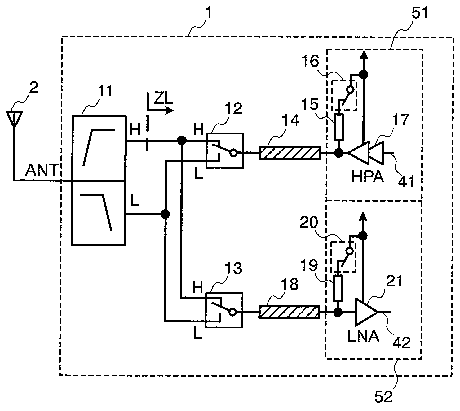
[0023]In FIG. 1, a reference numeral 1 depicts a high-frequency transmitting portion, which is built up with a Printed Circuit Board piling up a plural number of dielectric layers or films thereon, 2 an antenna, 11 a dividing filter (or, Diplexer), for letting a signal having frequency of 3,000 MHz or higher than that at an ANT terminal to pass through HPF (High Pass Filter) to a H terminal, while letting a signal of 900 MHz or lower than that to pass through a LPF (Low Pass Filter) to a L terminal, 12 and 13 band change-over switches, 17 a High Power Amplifier (HPA), 14 a wiring on the printed circuit board, for connecting a common terminal of the switch 12 and an output terminal of a HPA 17, 15 a reactance element, which can change an impedance (shown by “ZL” in FIG. 1) of the d...

embodiment 2

[0049]FIG. 6 shows the multi-mode wireless receiver, according to an embodiment 2 of the present invention. In this FIG. 6, comparing to that shown in FIG. 1, it differs from the embodiment 1 shown in FIG. 1, in that an impedance matching circuit 31 for the HPA of the diplexer 11 and an impedance matching circuit 32 for the LPF of the diplexer 11 are added, i.e., the impedance (shown by “ZL” in FIG. 6) when seeing the HPA 17 from the H terminal of the diplexer 11.

[0050]On the side of the H terminal of the HPF, an impedance can be matched to the pass-band, and in more details thereof, it can be achieved by means of a T-type matching circuit, a π-type matching circuit, or a L-type matching circuit.

[0051]The high power amplifier 17, the reactance element, and the switch 16 to be turned ON / OFF, so that the reactance element 15 gives an influence upon the output impedance of the HPA, are constructed as an unit, on a semiconductor integrated circuit 61, and the low noise amplifier 21, the...

embodiment 3

[0055]FIG. 7 shows a multi-mode wireless receiver, according to an embodiment 3 of the present invention. In this FIG. 7, the reference numeral 1 depicts the high-frequency transmitting portion of the first embodiment, but a reference numeral 3 depicts a software defined wireless signal processing portion, 4 a software defined wireless receiver, 43 a D / A converter, 41 a transmitting signal to be outputted by the D / A converter, 44 an A / D converter, 42 a receiving signal to be inputted into the A / D converter, and 45 a signal processing portion for conducting demodulation and / or enclosing / decoding therein.

[0056]The software defined wireless signal processing portion 3 conducts a software defined wireless signal process, which is proposed for achieving the wireless systems, differing in the frequency band, the multiplex accessing method, the signal Duplexing method, the modulation / demodulation method, the encoding / decoding method, such as, the portable telephones method and the wireless...


PUM


Abstract

When switching over from a portable telephone system of 800 MHz band to a UWB communication system of 9 GHz band, depending upon a signal for changing over a high pass filter and a low pass filter, a reactance element, which is determined to be matching with a load Z of the high pass filter, is connected to an output terminal of a transmitting power amplifier. With this, it is possible to achieve a multi-band or multi-mode wireless receiver of using a frequency band from 800 MHz to 10 GHz, without an enlargement of a circuit scale and an increase of costs.

Description

BACKGROUND OF THE INVENTION[0001]This invention relates to a compound wireless device of multi-band or multi-mode, for enabling to deal with different wireless systems, with using a plural number of frequency bands, and in particular, it relates to a semiconductor integrated circuit for use in a wireless device of Ultra Wide Band (UWB) method having wide band, such as, 9,504 MHz at the maximum frequency, and also in a multi-band wireless device.[0002]In a wireless local area network (hereinafter, “wireless LAN”), there is proposed a system for frequency hopping between frequency bands at high speed, so as to build up a frequency band of wide band signal with using a multi-carrier method for achieving a high transmitting speed, as well as, for spreading signal spectrum thereof.[0003]In more details, an Ultra Wide Band (hereinafter, “UWB”) system is proposed as a 802.15a standard of IEEE of U.S.A., applying an Orthogonal Frequency Division Multiplexing (hereinafter, “OFDM”) into the m...

Claims


Application Information

Patent Timeline
Patent Type & Authority Applications(United States)
IPC IPC(8): H04B1/06H03F1/56H04B1/44H04B1/50H04B1/713H04J11/00
CPCH03F1/22H03F1/565H03F3/195H03F3/24H03F2200/108H03F2200/111H03F2200/75H03F2200/381H03F2200/387H03F2200/391H03F2200/451H03F2200/519H03F2200/294
Inventor SUGIYAMA, YOSHIKAZUADACHI, SATOSHIKATSUBE, YUSAKUTONE, MASAZUMITAKAKI, TAKU
Owner HITACHI MEDIA ELECTORONICS CO LTD
Why Eureka
Try Eureka