Integrated Circuit Package and a Method for Forming an Integrated Circuit Package

a technology of integrated circuits and components, applied in the direction of electrical equipment, semiconductor devices, semiconductor/solid-state device details, etc., can solve the problems of limiting the improvement that can be achieved, the moisture resistance of the package is increased, and the electrical connection between the chip and the substrate is not working properly, so as to reduce the mechanical strength of the assembly, improve the moisture resistance of the package, and reduce the performance of the underfill layer. effect of function

Inactive Publication Date: 2008-05-29
INFINEON TECH AG
View PDF11 Cites 8 Cited by
  • Summary
  • Abstract
  • Description
  • Claims
  • Application Information

AI Technical Summary

Benefits of technology

[0010]The present inventors have found that popcorn-delamination in Flip Chip packages initiates from the center of the package, and progresses towards the edge of the package. By providing an area around the center of the package in which no underfill material is present, the possibility for delamination between the chip and the underfill layer in this central region can be avoided. By elimination of the initiation site, it is believed that the moisture performance of the package can be improved.
[0011]It has been found that the absence of underfill material in the center region of the package does not result in a significant decrease in the performance of the functions of the underfill layer, in particular that this does not significantly decrease the mechanical strength of the assembly, or the ability to compensate for thermal expansion differences between the chip and substrate. Further, since the underfill material can still encapsulate the bumps connecting the chip and substrate, the underfill material is still able to protect the bumps from moisture or other environmental hazards.
[0012]The central void can be provided using a seal pass, in which the underfill material is provided along each side of the chip, entrapping the central void. In one example, the seal pass is carried out quickly so that a volume of air or other ambient gas is trapped under the center of the chip preventing the underfill material from flowing into the central void. The fast seal-pass is important when the underfill material has a low viscosity. Alternatively or additionally, the underfill material may have a high viscosity, for example, a viscosity of at least 50 Pa.s. In this case, a seal-pass method is again used to deposit the underfill material along each side of the chip. However, the use of a material of high viscosity minimizes the flow rate of the material, and therefore reduces the need for the seal-pass to be carried out at high speed. By using an underfill material with a high filler loading, for example, with a filler loading of at least 75%, the material will have a sufficiently high viscosity to avoid the need for the seal-pass to be completed quickly. An additional advantage of using a material with a high filler loading is that the material will have improved moisture characteristics.

Problems solved by technology

One problem with known Flip Chip packages is their susceptibility to moisture attack, and in particular “popcorn-delamination” whereby moisture can cause the delamination of the chip, underfill layer and substrate.
Such delamination can result in the failure of the electrical connection between the chip and substrate.
However, there is a limit in the improvements that can be achieved merely by selection of materials and improvement of the adhesion.

Method used


Image

  • Integrated Circuit Package and a Method for Forming an Integrated Circuit Package
  • Integrated Circuit Package and a Method for Forming an Integrated Circuit Package
  • Integrated Circuit Package and a Method for Forming an Integrated Circuit Package

Examples


Embodiment Construction

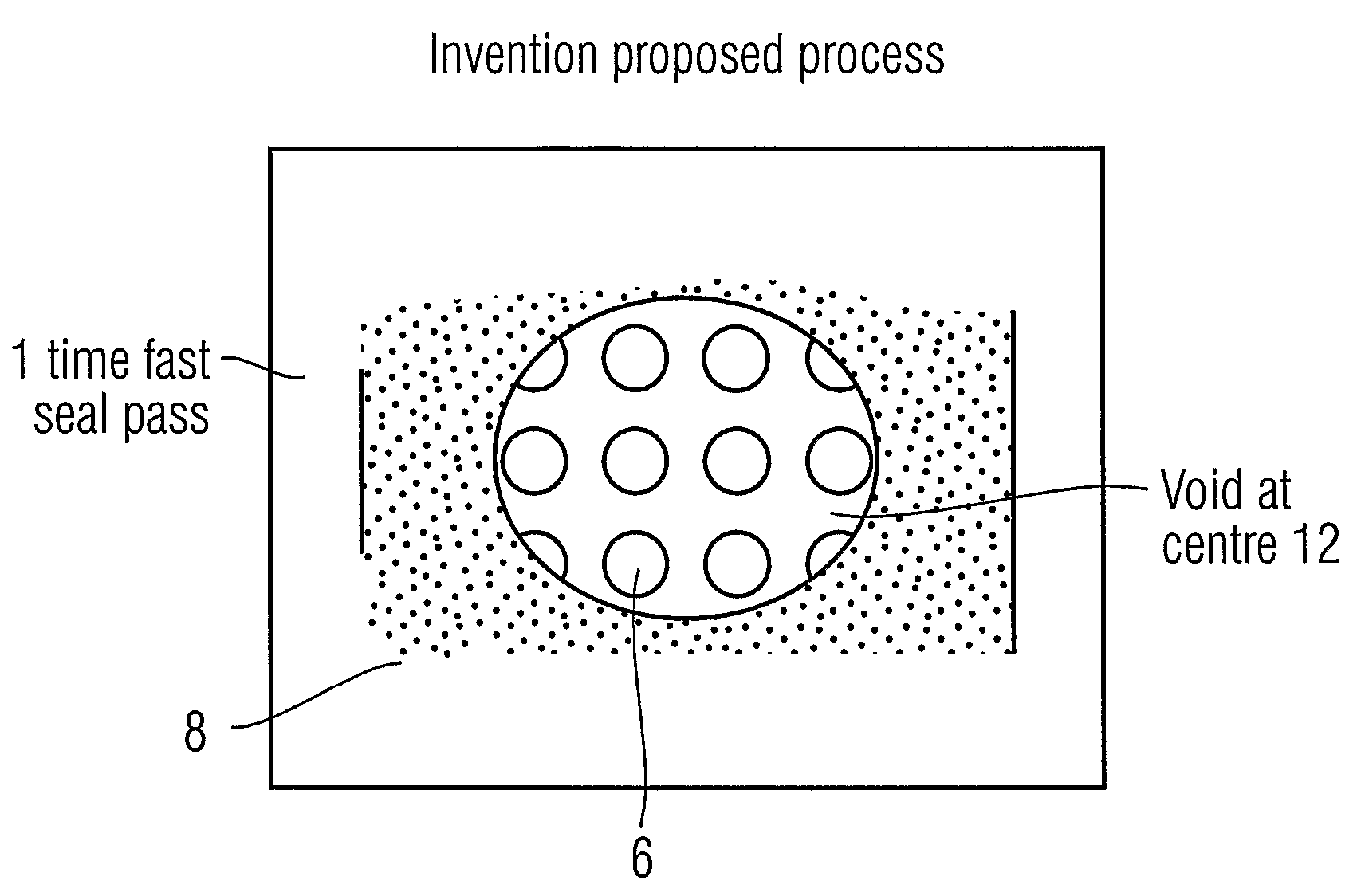
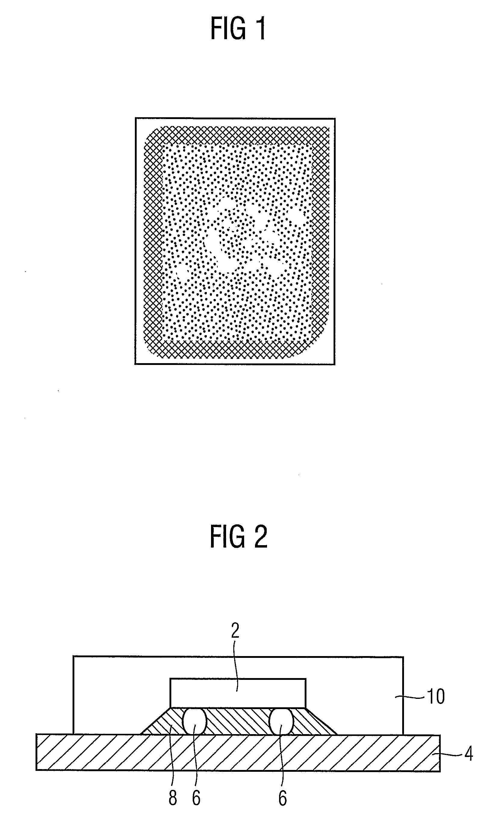
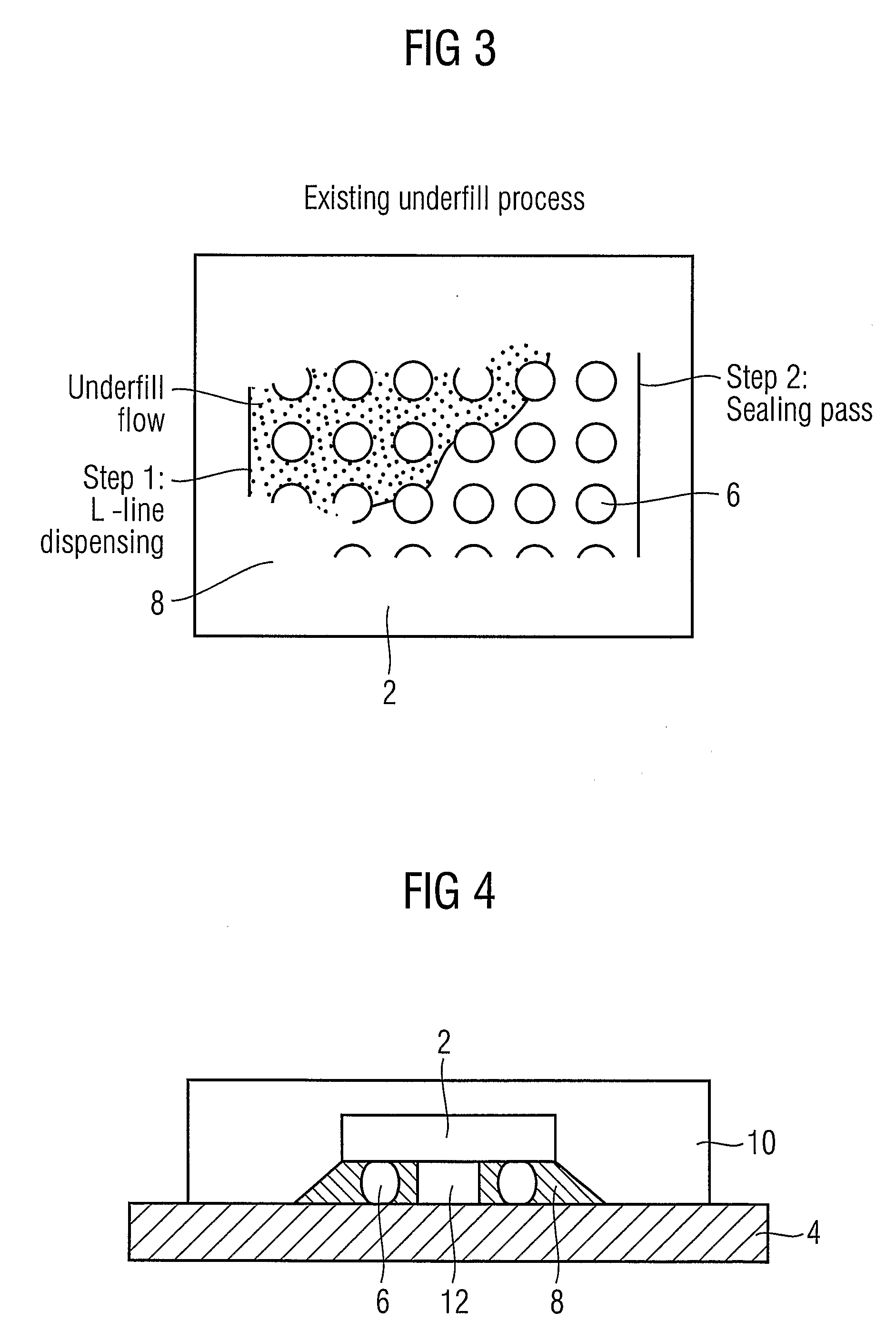
[0022]A conventional Flip Chip package will be described with respect to FIGS. 2 and 3.

[0023]As shown in the cross-section of FIG. 2, a chip 2 is mounted on a substrate, carrier or circuit board 4 by means of conductive bumps 6. In a typical example, the bumps 6 are formed by sputtering, plating or printing a solderable material on the chip 2, and these are connected and soldered to chip bond pads provided on the substrate 4.

[0024]A non-conductive underfill layer 8 is provided under the chip 2. As can be seen in FIG. 2, the underfill material surrounds the bumps 6, and fills the entire region underneath the chip between the chip and the substrate. Typically the underfill extends beyond the outer periphery of the chip. It is typical to provide the underfill material by dispensing the material along one or two sides of the periphery of the chip, allowing the material to flow under the chip to fill the area between the chip and substrate. Where material is deposited along one side only...


PUM


Abstract

A method of forming an integrated circuit package, such as a Flip Chip package, in which a void is provided in the underfill material in the central region of the package between the chip or die and the substrate on which the chip or die is mounted. This reduces delamination of the package as a result of moisture.

Description

[0001]This application is a continuation of co-pending International Application No. PCT / SG2005 / 000270, filed Aug. 4, 2005, which designated the United States and was published in English of which application is incorporated herein by reference.TECHNICAL FIELD[0002]The present invention relates to a method of manufacturing an integrated circuit package, and to an integrated circuit package manufactured according to the method. In particular, embodiments of the invention relate to a Flip Chip (FC) or Direct Chip Attach (DCA) package in which the chip is attached directly to the substrate, board or carrier by conductive bumps.BACKGROUND[0003]In integrated circuit packages, the electronic components are mounted on a substrate, circuit board or carrier. The electrical connection between the components and the substrate can be achieved through wire bonds, or through connecting bumps, such as solder bumps. The chip, substrate and interconnection are typically encapsulated to produce the f...

Claims


Application Information

Patent Timeline
Patent Type & Authority Applications(United States)
IPC IPC(8): H01L23/02
CPCH01L21/563H01L23/3121H01L2224/73203H01L2924/01078H01L2224/16225H01L2224/32225H01L2224/73204H01L2924/00
Inventor OFNER, GERALDYEO, SWAIN HONGTEO, MARYLIM, PEI SIANGCHUA, KHOON LAM
Owner INFINEON TECH AG
Why Eureka
Try Eureka