Light-emitting device and manufacturing method thereof

a technology of light-emitting devices and manufacturing methods, which is applied in the manufacture of electrode systems, electric discharge tubes/lamps, and discharge tubes luminescent screens, etc., can solve the problems of increasing the tone unevenness of light passing through the optical element, the inability of phosphors to be thinly and uniformly disposed around the light-emitting element b>5, and the increase of the tone unevenness of light collected by the optical lens. , to achieve the effect o

Inactive Publication Date: 2008-05-29
DOWA ELECTRONICS MATERIALS CO LTD
View PDF4 Cites 47 Cited by
  • Summary
  • Abstract
  • Description
  • Claims
  • Application Information

AI Technical Summary

Benefits of technology

[0022]According to the present invention, the use of the light-emitting element whose main emission wavelength is equal to or less than 410 nm not falling within a visible spectrum makes it possible to lower directivity of visible light emitted by the light-emitting device, and fixing the phosphor layer to the adhesive whose thickness is equal to or less than the average particle size of the phosphors makes it possible to uniformly distribute the phosphors in the phosphor layer, enabling further reduction in tone unevenness.

Problems solved by technology

However, in a case where the light-emitting device 100 described in the aforesaid Japanese Patent Application Laid-open No. 2001-127346 is used, since the phosphors are mixed in transparent resin to cover the light-emitting element, the phosphors cannot be thinly and uniformly disposed around the light-emitting element 5 due to surface tension of the mixed solution, and the phosphors settle in the mixed solution in a curing process of the resin.
Due to the influence of these, tone unevenness is not fully solved, resulting in increased tone unevenness of the light gathered by the optical lens 102.
Further, the use of an optical element such as a lens for gathering and scattering light results in increased tone unevenness of light having passed through the optical element because blue light emitted by the light-emitting element has directivity.
Consequently, equipment space and equipment cost are increased and in addition, there occurs color unevenness in the gathered light because the distribution by the light diffuser is not uniform, which has made it difficult to form a light-emitting element with uniform color temperature.

Method used


Image

  • Light-emitting device and manufacturing method thereof
  • Light-emitting device and manufacturing method thereof
  • Light-emitting device and manufacturing method thereof

Examples


example 1

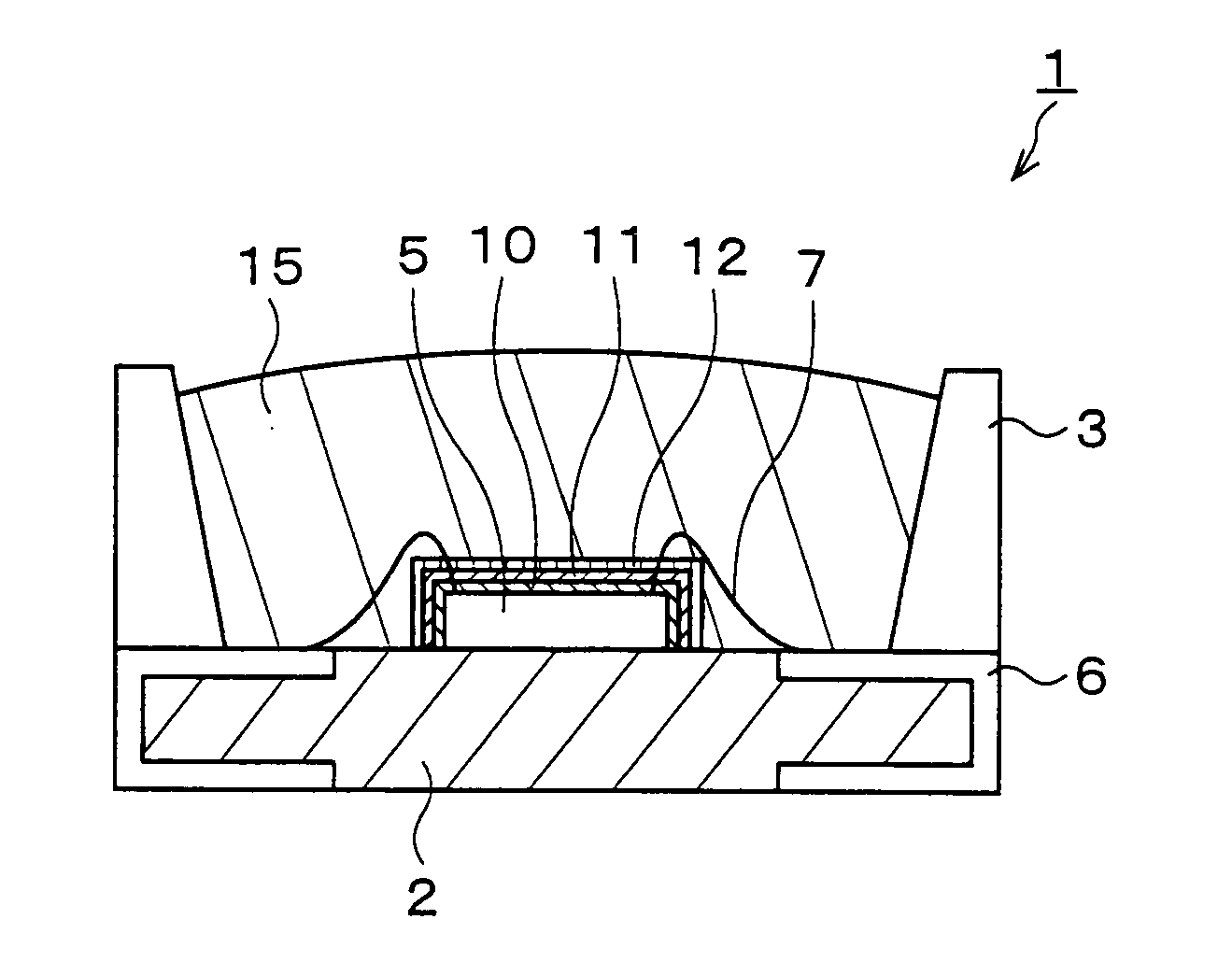
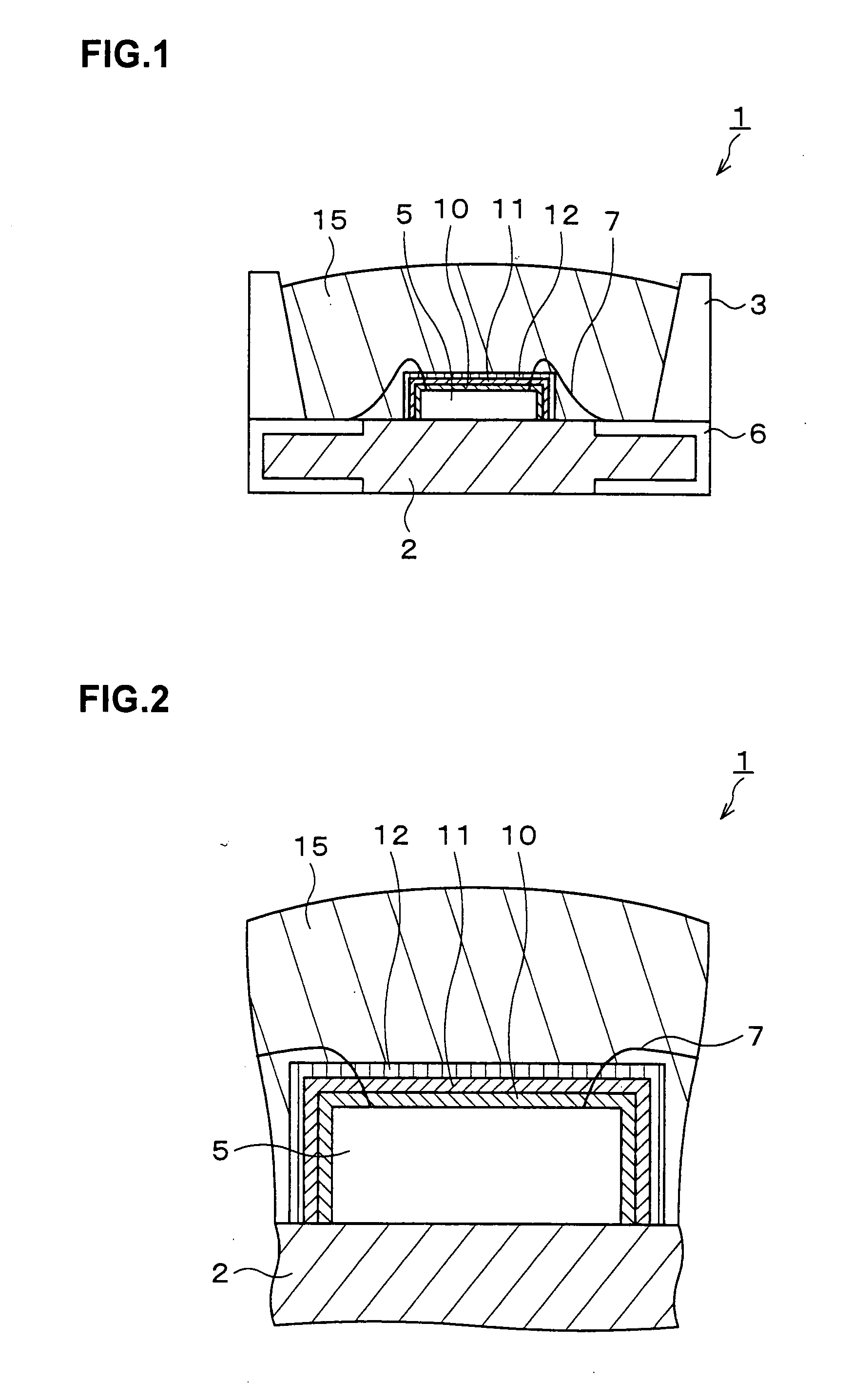
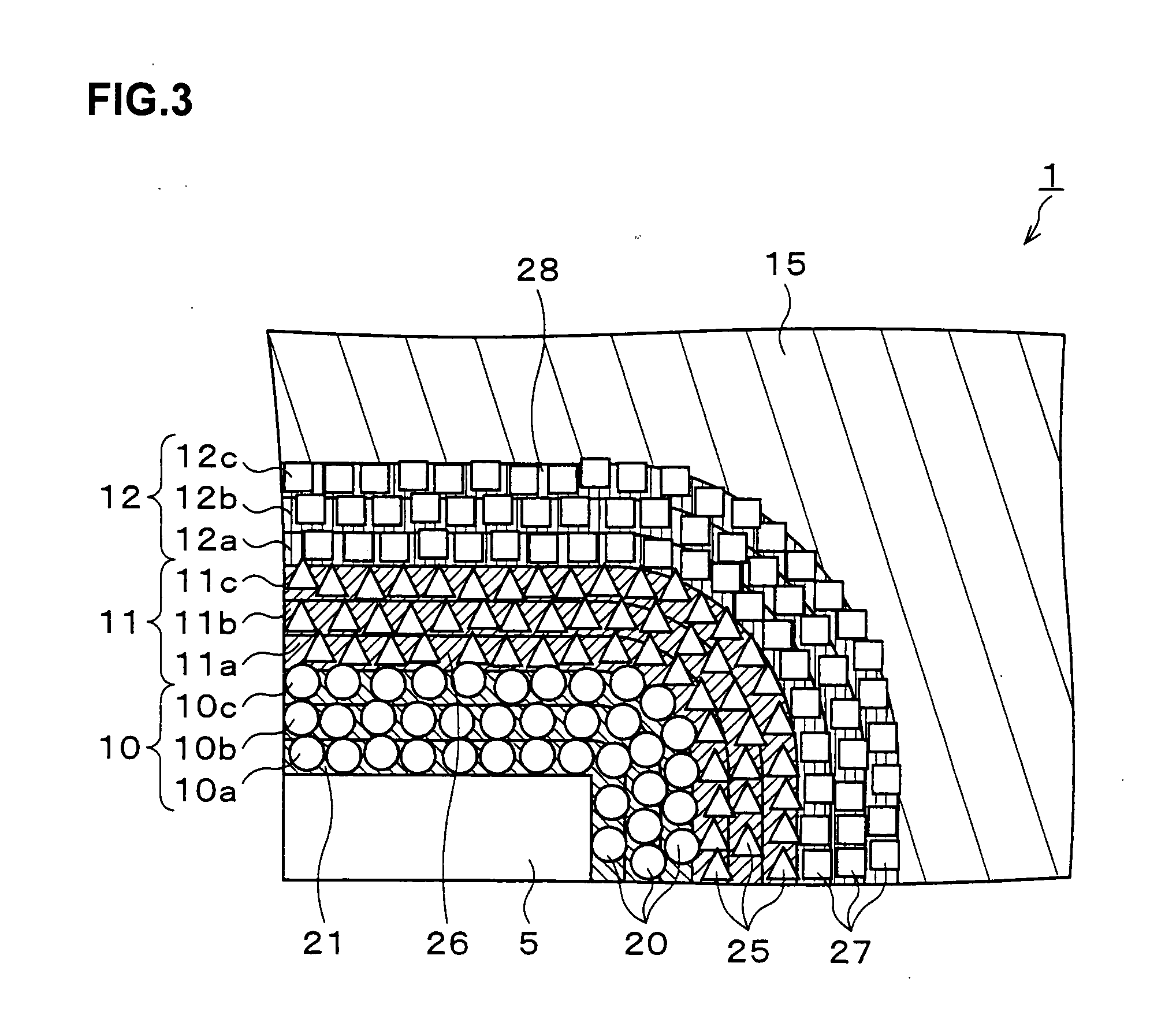
[0105]The light-emitting device 1 shown in FIG. 2 was formed in which the three different phosphor layers 10, 11, 12 were stacked directly on the light-emitting element 5 emitting ultraviolet light whose main emission wavelength was 405 nm. In the example 1, CaAlSiN3:Eu was used as the phosphors 20 contained in the phosphor layer 10, SrAl1+xSi4−xOxN7−x:Ce was used as the phosphors 25 contained in the phosphor layer 11, and SrAlxSi6−xO1+xN8−x:Eu was used as the phosphors 27 contained in the phosphor layer 12. A particle size of the phosphors 20 was adjusted to 10 μm or less, a particle size of the phosphors 25 was adjusted to 13 μm or less, and a particle size of the phosphors 27 was adjusted to 20 μm or less.

[0106]When a cross section of the above sample was observed, occupancy ratios of the phosphors 20, the phosphors 25, and the phosphors 27 in the phosphor layer 10, the phosphor layer 11, and the phosphor layer 12 were all 50% or more, specifically 60%. Thickness variation (diffe...


PUM


Abstract

A light-emitting device includes: a light-emitting element whose main emission wavelength is 410 nm or less; and one phosphor layer or more stacked to cover a light-emitting surface of the light-emitting element and containing phosphors that absorb light from the light-emitting element and wavelength-convert the absorbed light to emit light.

Description

BACKGROUND OF THE INVENTION[0001]1. Field of the Invention[0002]The present invention relates to a light-emitting device emitting white light, which is used as, for example, an illumination light source, a light source of a backlight of a liquid crystal display, and relates to a manufacturing method thereof.[0003]2. Description of the Related Art[0004]In recent years, a light-emitting device has been developed which emits white light having a wide emission wavelength interval by combining a light-emitting element which emits ultraviolet light or blue light and phosphors which absorb the light from the light-emitting element and wavelength-convert the absorbed light to emit long-wavelength light. Such a light-emitting device is used as, for example, an illumination light source, a light source of a backlight of a liquid crystal display, and the like. In the application to an illumination light source and a light source of a backlight of a liquid crystal display, there is a demand for...

Claims


Application Information

Patent Timeline
Patent Type & Authority Applications(United States)
IPC IPC(8): H01J1/62H01J9/02H01L33/50H01L33/54H01L33/62
CPCH01J1/63H01L33/44H01L33/501H01L33/504H01L2224/8592H01L2933/0041H01L2224/48091H01L2924/00014H01L2924/181H01L2924/00012
Inventor MARUYAMA, TSUKASAIKUTA, TETSUYA
Owner DOWA ELECTRONICS MATERIALS CO LTD
Why Eureka
Try Eureka