

Semiconductor memory device
a memory device and semiconductor technology, applied in static storage, digital storage, instruments, etc., can solve the problems of reducing the sum of gidl current flowing through the pmos transistor of all sub-word drivers, too large to ignore, and suppressing gidl current, so as to reduce the current of the semiconductor memory device, and reduce the effect of gidl curren
- Summary
- Abstract
- Description
- Claims
- Application Information
AI Technical Summary
Benefits of technology
Problems solved by technology
Method used
Image

Examples
Embodiment Construction
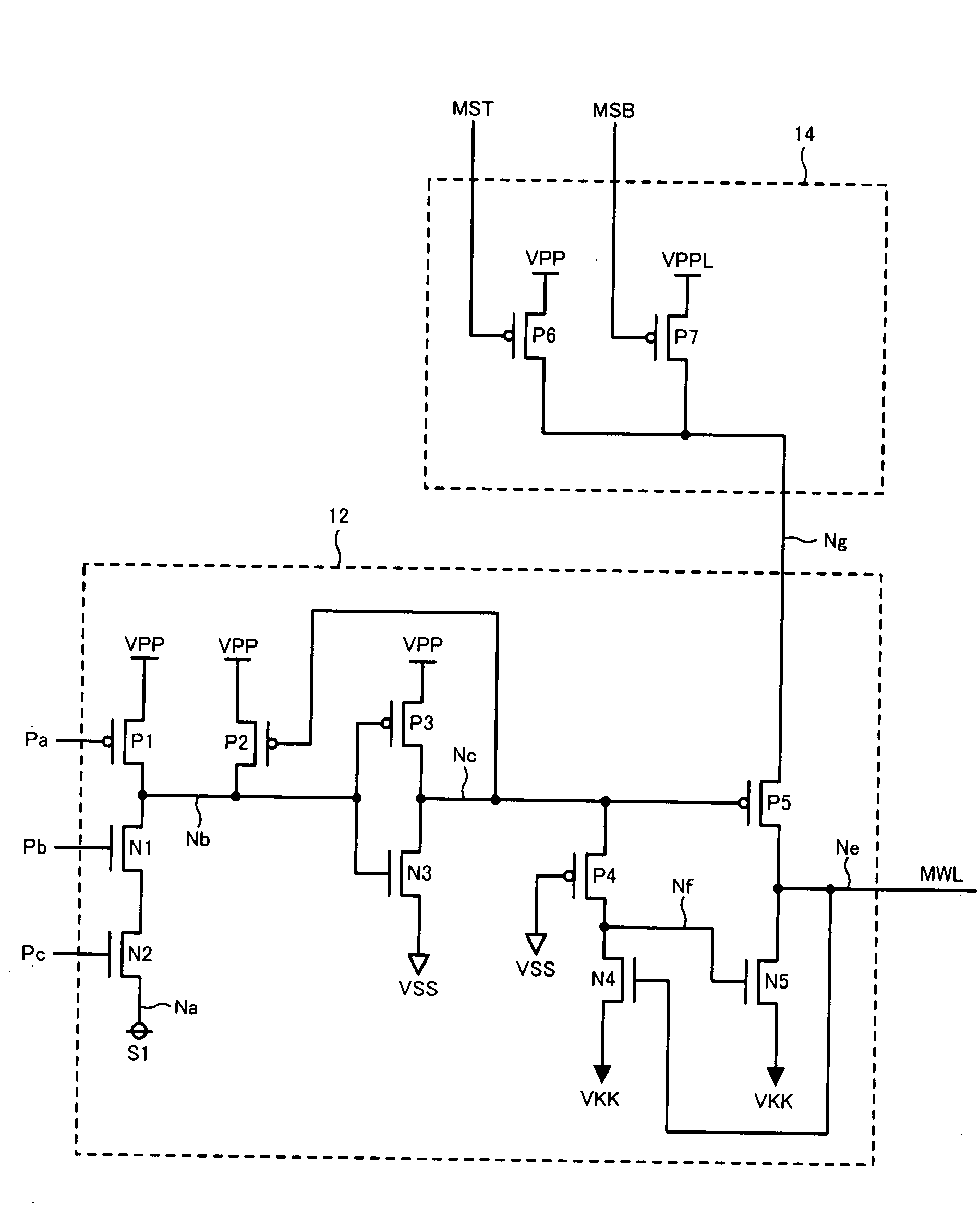
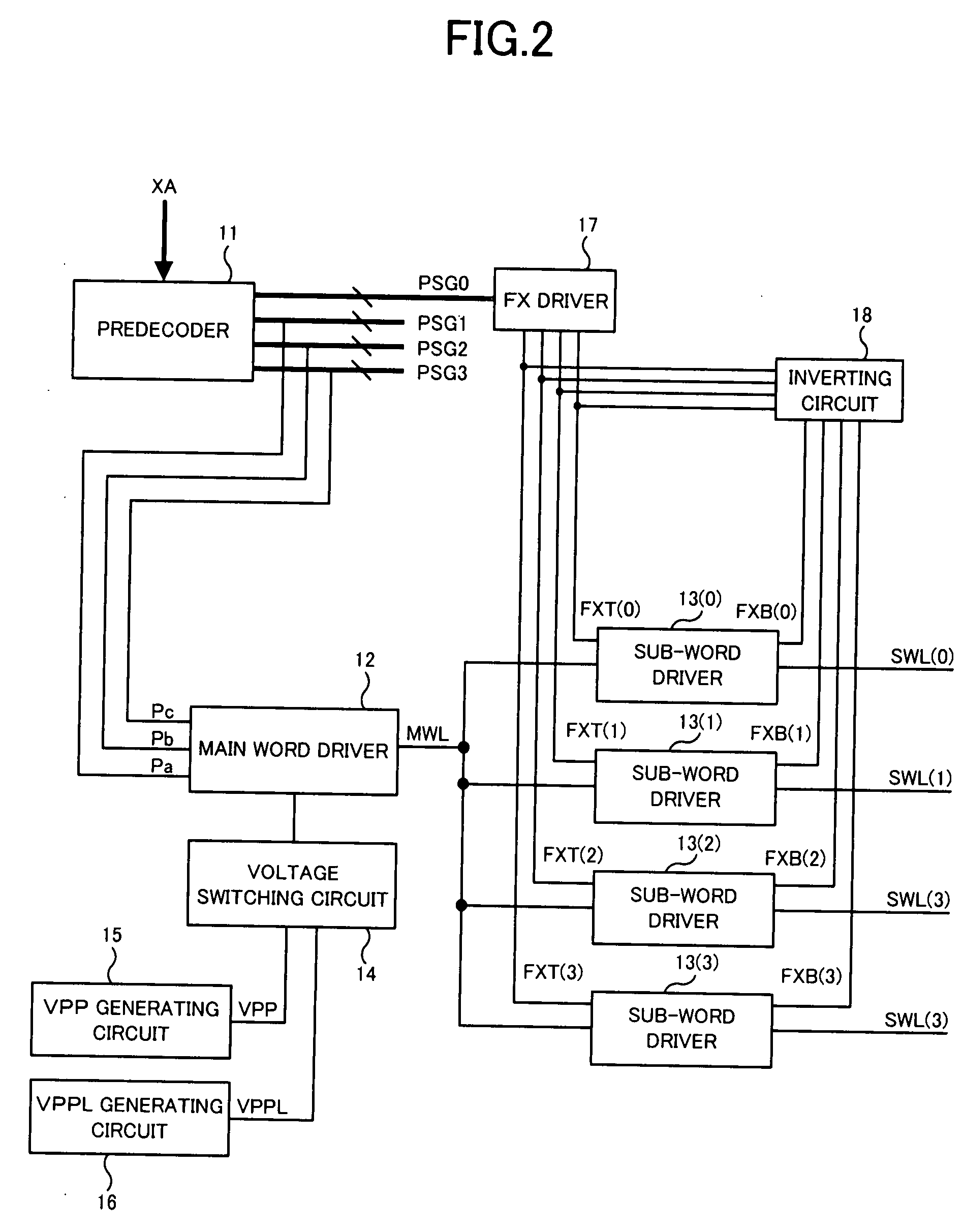
[0027]Hereinafter, an embodiment of the present invention is described with reference to the drawings. In this embodiment, the description is given about a case where the present invention is applied to a DRAM having a hierarchical word line structure including a plurality of main word lines and a plurality of sub-word lines.
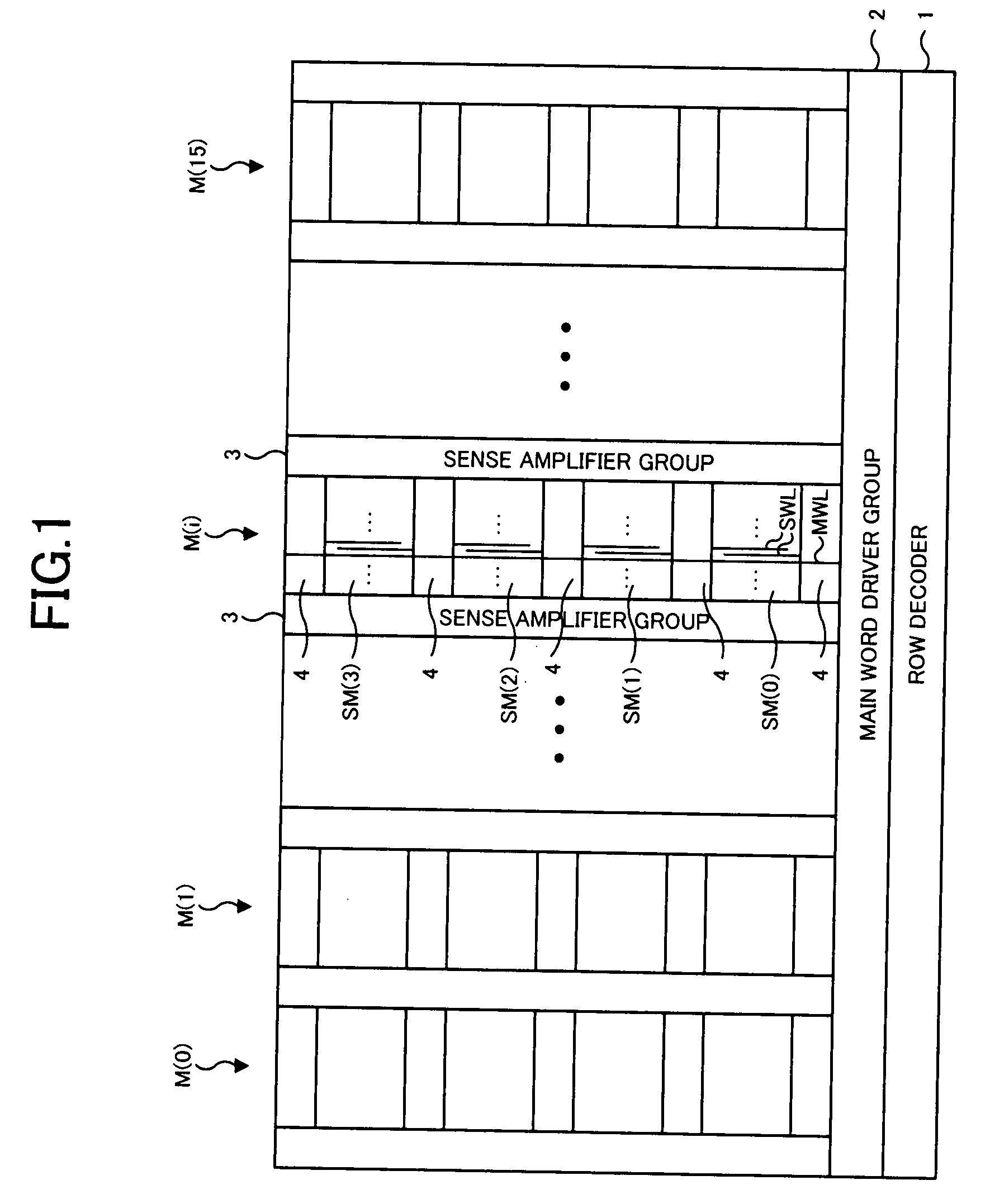
[0028]FIG. 1 shows an entire configuration of the DRAM of the embodiment. As shown in FIG. 1, the DRAM of the embodiment includes a plurality of memory mats M into which a memory cell array including many memory cells is divided for every predetermined number of main word lines, a row decoder 1 for outputting a decode signal corresponding to the hierarchical word line structure based on an input row address, a main word driver group 2 including many main word drivers for activating main word lines selected by the row decoder 1, sense amplifier groups 3 each including many sense amplifiers for amplifying data read from the memory cells of each memory mat M, and s...
PUM
 Abstract
Description
Claims
Application Information