This helps you quickly interpret patents by identifying the three key elements:
Problems solved by technology
Method used
Benefits of technology
[0026]In preferred embodiments the photodiode layer is a single three-layer photodiode layer of charge generating material located above the pixel circuits convert electromagnetic radiation into electrical charges. This photodiode layer comprises an n-layer, and i-layer and a p-layer. The photodiode layer is laid over the top of the pixel circuitry. By laying the photodiode structure over the pixel readout circuitry, the resulting sensor has a near-unity (substantially 100 percent) fill factor. This feature results in near unity quantum efficiency for specific wavelength bands. This provides a distinct advantage over a front-illuminated charge-coupled device or conventional CMOS imagers, both which effectively shield a la
Problems solved by technology
The photoresponse of these sensors is typically limited to the 400 nm-900 nm spectral range by the semiconductor bandgap properties of crystalline silicon.
Also, in prior art CMOS sensors, the CMOS pixel circuitry obscures a major portion of each pixel's photosensitive area, resulting in low collection efficiency.
But at some point depending on the number of pixels on which the target region has been imaged, the pixels begin to appear as squares or re
Method used
Image
Click on the blue label to locate the original text in one second.
Reading with bidirectional positioning of images and text.
Examples
Embodiment Construction
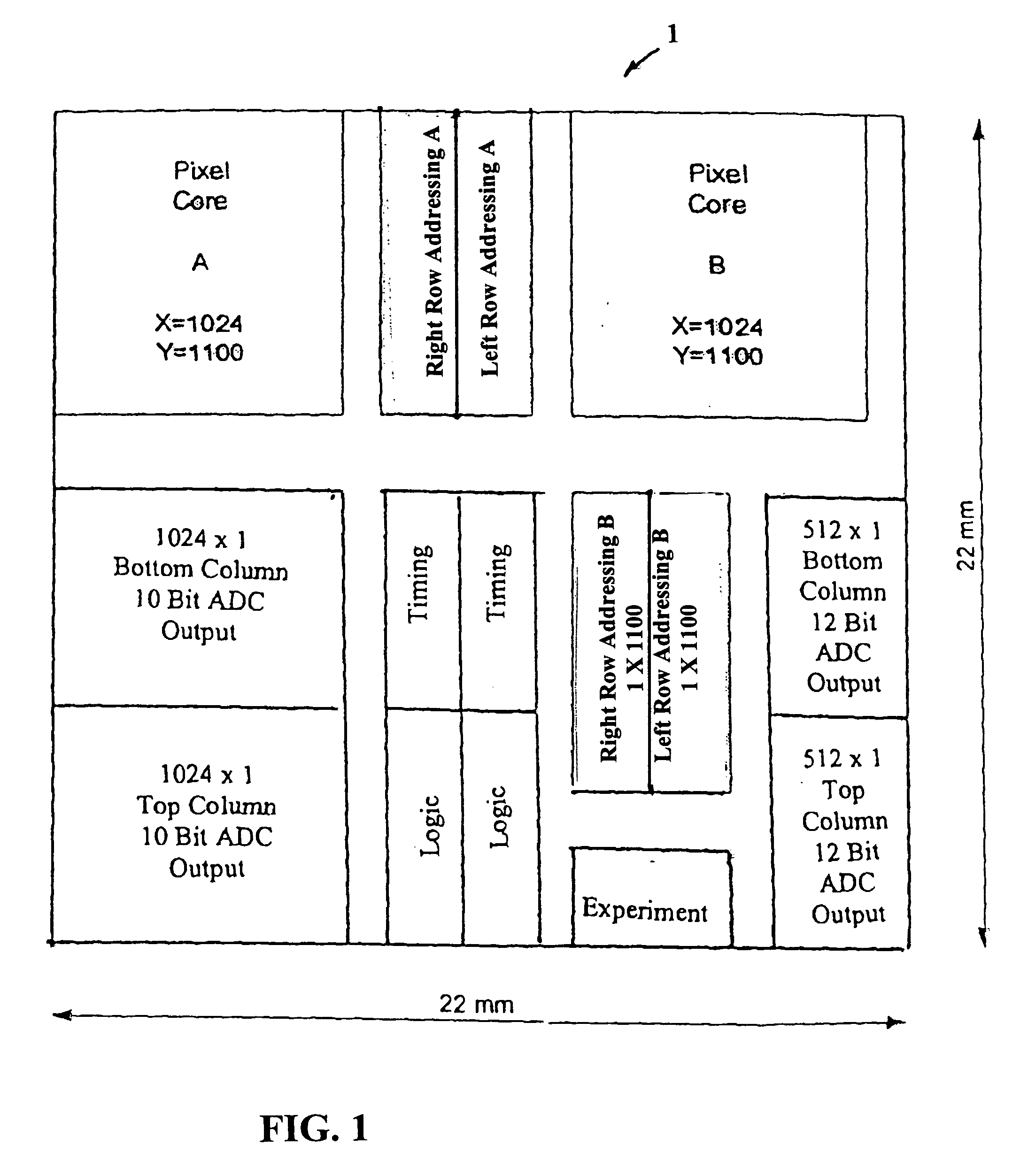
Many Million Pixel Sensors
[0047]The present invention provides CMOS sensors having a single continuous photodiode layer covering a pixel circuit array with at least about 25 million pixels. In preferred embodiments pixel sizes range from about 1.75 microns to 7.5 microns. Current standard pixel sizes are 1.75 microns, 3 microns, 5 microns and 7.5 microns. Applicants have fabricated and tested a sensor with 36 million 7.5 micron pixels and have described detailed designs for a much larger pixel with pixel counts as high as 250 million pixels or greater.
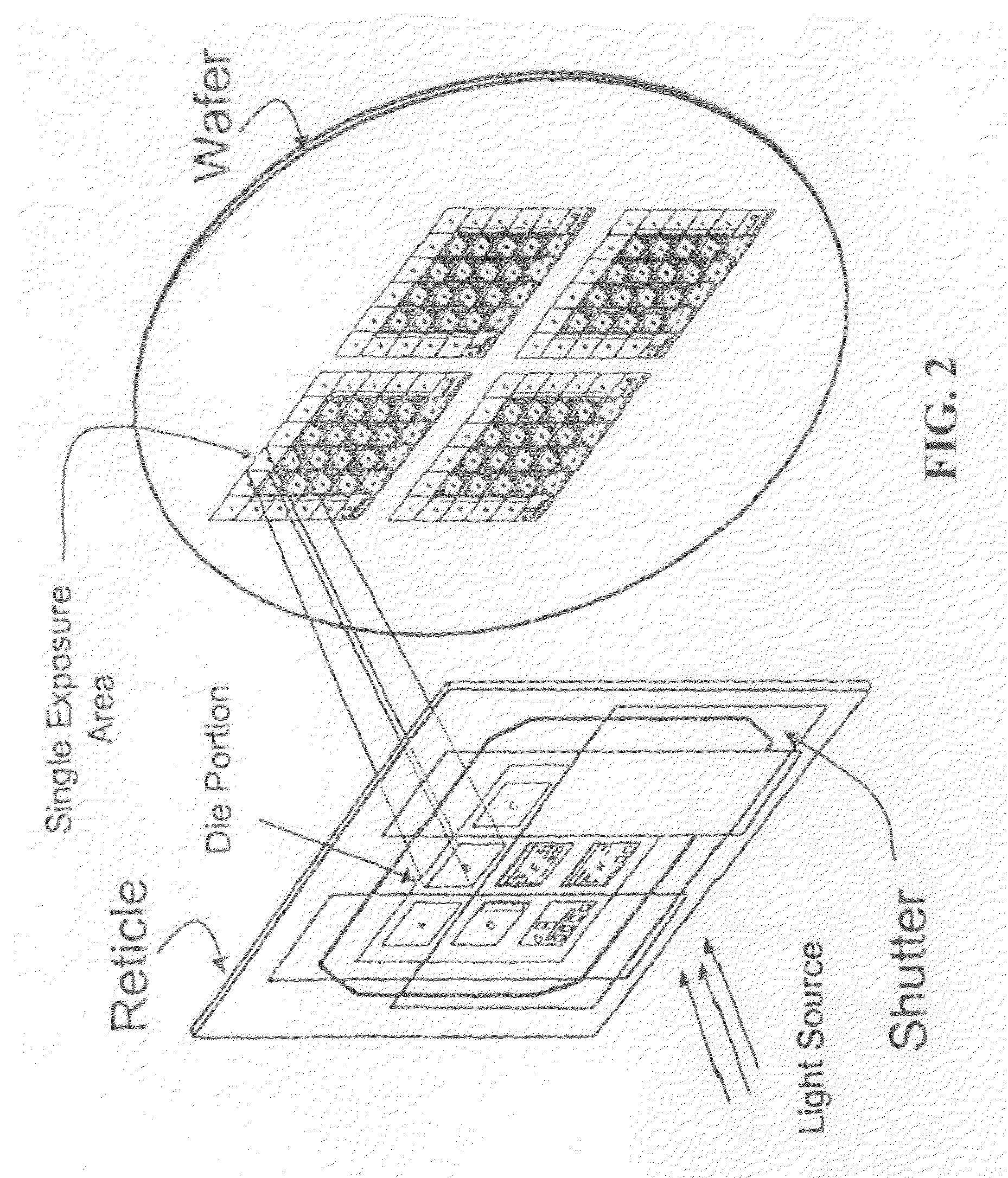
CMOS Lithographic Stitching for Very Large Pixel Arrays
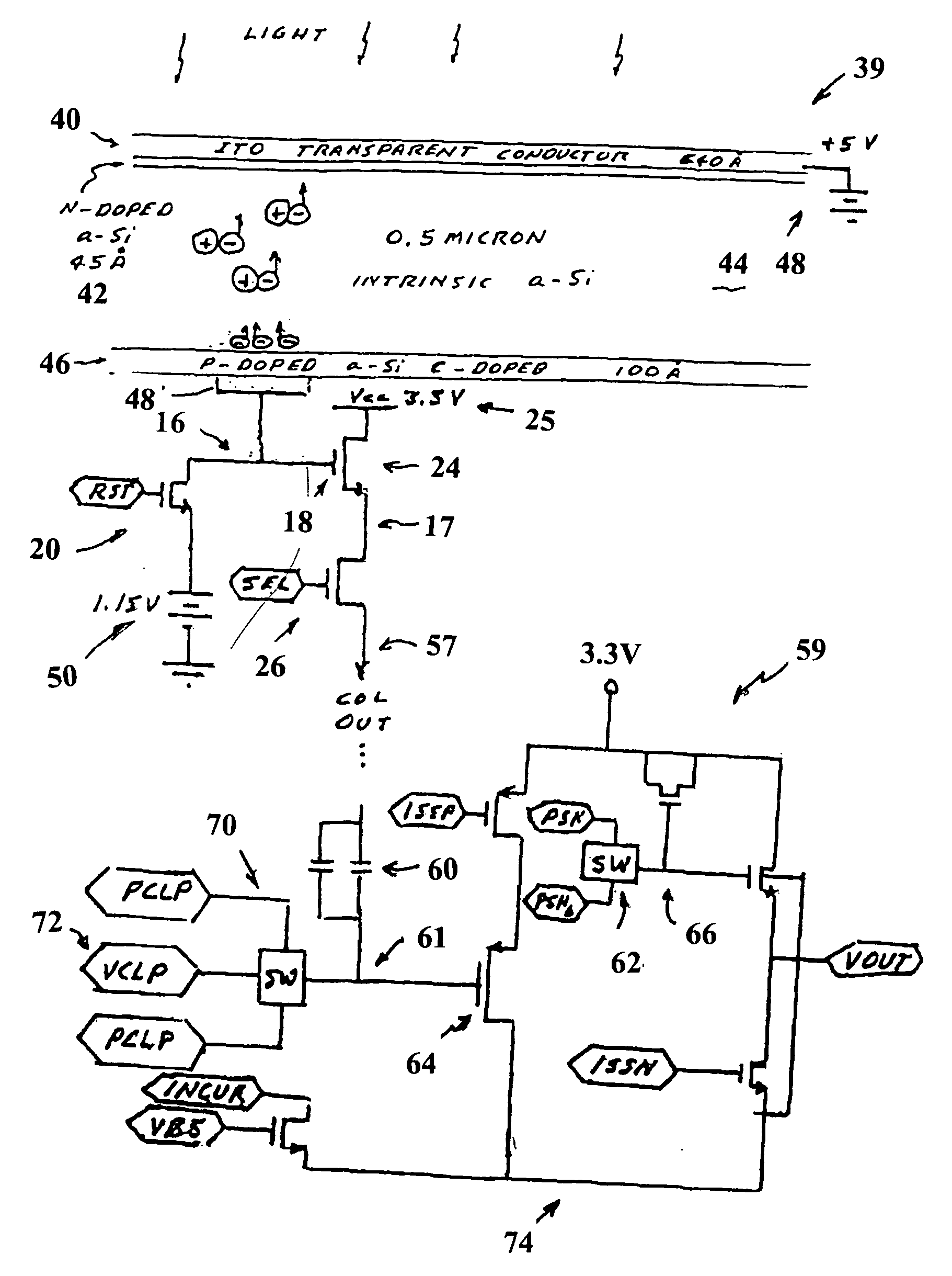
[0048]In the parent patent applications listed in the first sentence of this application, Applicants and their fellow workers describe in detail Applicant's proprietary process of fabricating CMOS sensors by depositing a single continuous multi-layer photodiode layer on top of an array of pixel circuits to provide substantially 100 percent packing factor and minimize pixel sizes. A...
PUM
Abstract
A CMOS image sensor with a many million pixel count. Applicants have developed techniques for combining its continuous layer photodiode CMOS sensor technology with CMOS integrated circuit lithography stitching techniques to provide digital cameras with an almost unlimited number of pixels. A preferred CMOS stitching technique exploits the precise alignment accuracy of CMOS stepper processes by using specialized mask sets to repeatedly produce a single pixel array pattern many times on a single silicon wafer with no pixel array discontinuities. The single array patterns are stitched together lithographically to form a pixel array of many million pixels. A continuous multilayer photodiode layer is deposited over the top of the many million pixel array to provide a many million pixel sensor with a fill factor of 100 percent or substantially 100 percent.
Description
[0001]This application is a continuation in part of U.S. patent application Ser. No. 11 / 361,426 filed Feb. 24, 2006 and Ser. No. 10 / 185,833 filed Feb. 23, 2004 which was a continuation of patent application Ser. Nos. 10 / 746,529, filed Dec. 23, 2003; Ser. No. 10 / 648,129 filed Aug. 26, 2003, now U.S. Pat. No. 6,809,358; Ser. No. 10 / 371,618, filed Feb. 22, 2003, now U.S. Pat. No. 6,730,900; Ser. No. 10 / 229,953 filed Aug. 27, 2002; Ser. No. 10 / 229,954 filed Aug. 27, 2002, now U.S. Pat. No. 6,791,130; Ser. No. 10 / 229,955 filed Aug. 27, 2002; Ser. No. 10 / 229,956 filed Aug. 27, 2002, now U.S. Pat. No. 6,798,033 and Ser. No. 10 / 072,637 filed Feb. 5, 2002, now U.S. Pat. No. 6,730,914, all of which are incorporated herein by reference.[0002]The present invention was made in the course of work under Contract Number NRO000-04-C-0110 with an agency of the United States Government and, the United States Government has rights in the invention.[0003]This patent application relates to electronic ima...
Claims
Application Information
Patent Timeline
Application Date:The date an application was filed.
Publication Date:The date a patent or application was officially published.
First Publication Date:The earliest publication date of a patent with the same application number.
Issue Date:Publication date of the patent grant document.
PCT Entry Date:The Entry date of PCT National Phase.
Estimated Expiry Date:The statutory expiry date of a patent right according to the Patent Law, and it is the longest term of protection that the patent right can achieve without the termination of the patent right due to other reasons(Term extension factor has been taken into account ).
Invalid Date:Actual expiry date is based on effective date or publication date of legal transaction data of invalid patent.