Lcos display unit and method for forming the same

a display unit and liquid crystal technology, applied in the field of semiconductor devices, can solve the problems of increasing processing costs, increasing affecting the insulation performance of the mosfet, so as to increase the design area of a switch circuit, increase the capacitance, and reduce the refresh rate of the lcos display unit.

Active Publication Date: 2008-06-05
SEMICON MFG INT (SHANGHAI) CORP
View PDF31 Cites 27 Cited by
  • Summary
  • Abstract
  • Description
  • Claims
  • Application Information

AI Technical Summary

Benefits of technology

[0023]Compared with the prior art, the present invention has the following advantages: a Metal-Insulator-Metal (MIM) capacitor consisting of a micromirror layer, a insulation layer and a light shielding layer is formed by grounding the light shielding layer on a pixel switch circuit layer. Therefore the pixel switch circuit and the capacitor are in vertical distribution, that is, the switch circuit and the capacitor both have an allowable design area of the size of one pixel. Thus, the present invention makes

Problems solved by technology

As shown in FIG. 1, the capacitance is increased in the improved structure, but the processes are also increased, resulting in increased processing cost.
However, as restricted by the pixel area, if the capacitor occupies the pixel area i

Method used


Image

  • Lcos display unit and method for forming the same
  • Lcos display unit and method for forming the same
  • Lcos display unit and method for forming the same

Examples


Embodiment Construction

[0028]The above objects and advantages of the present invention will become more apparent with reference to the following description of the preferred embodiments given in conjunction with the accompanying drawings.

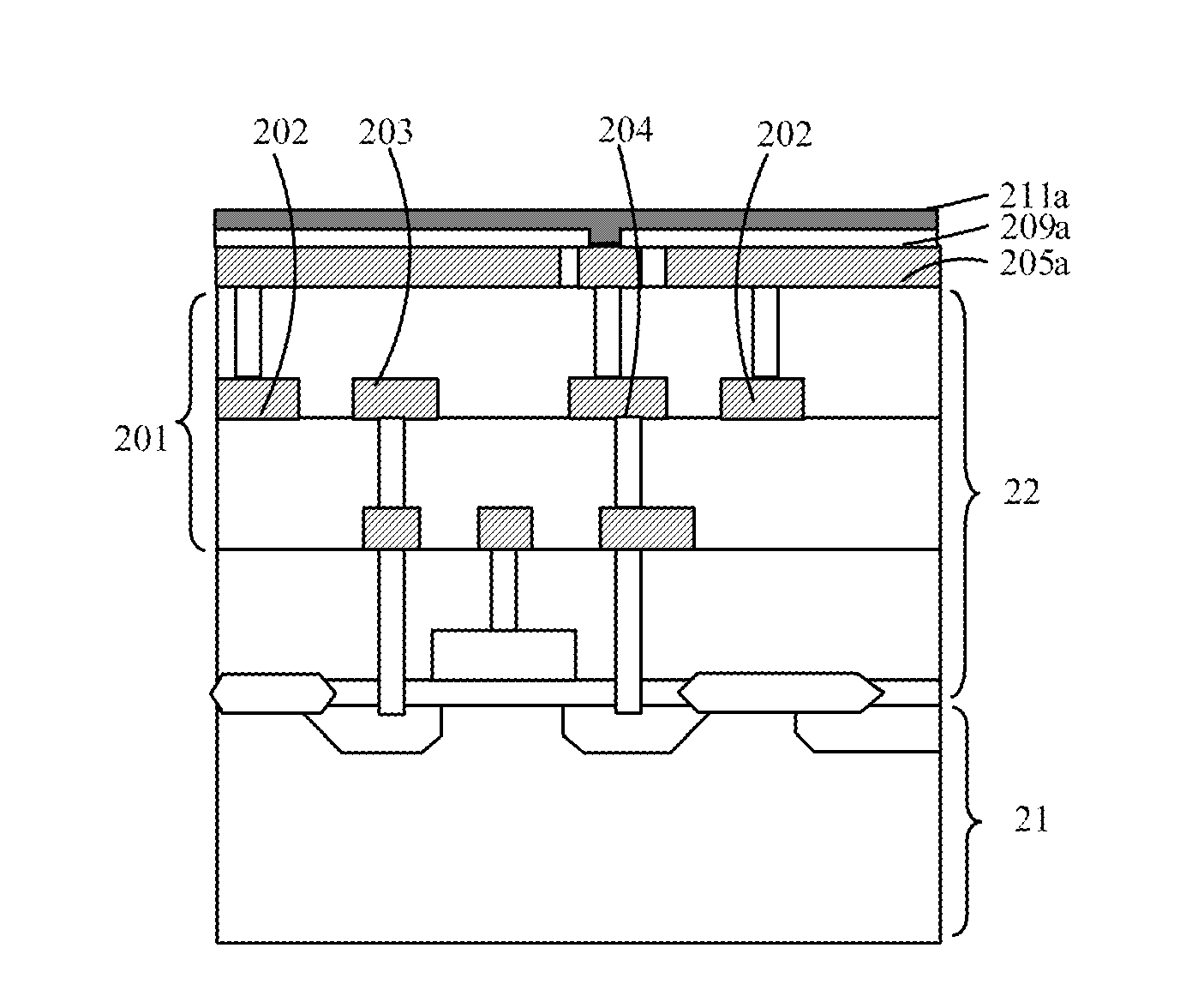
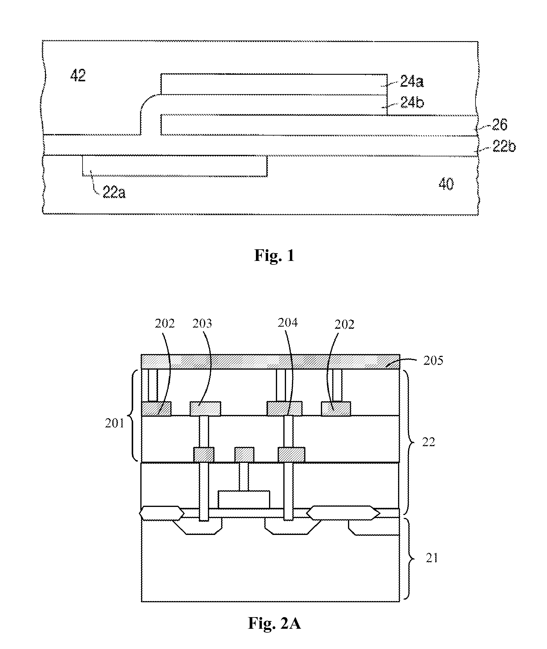
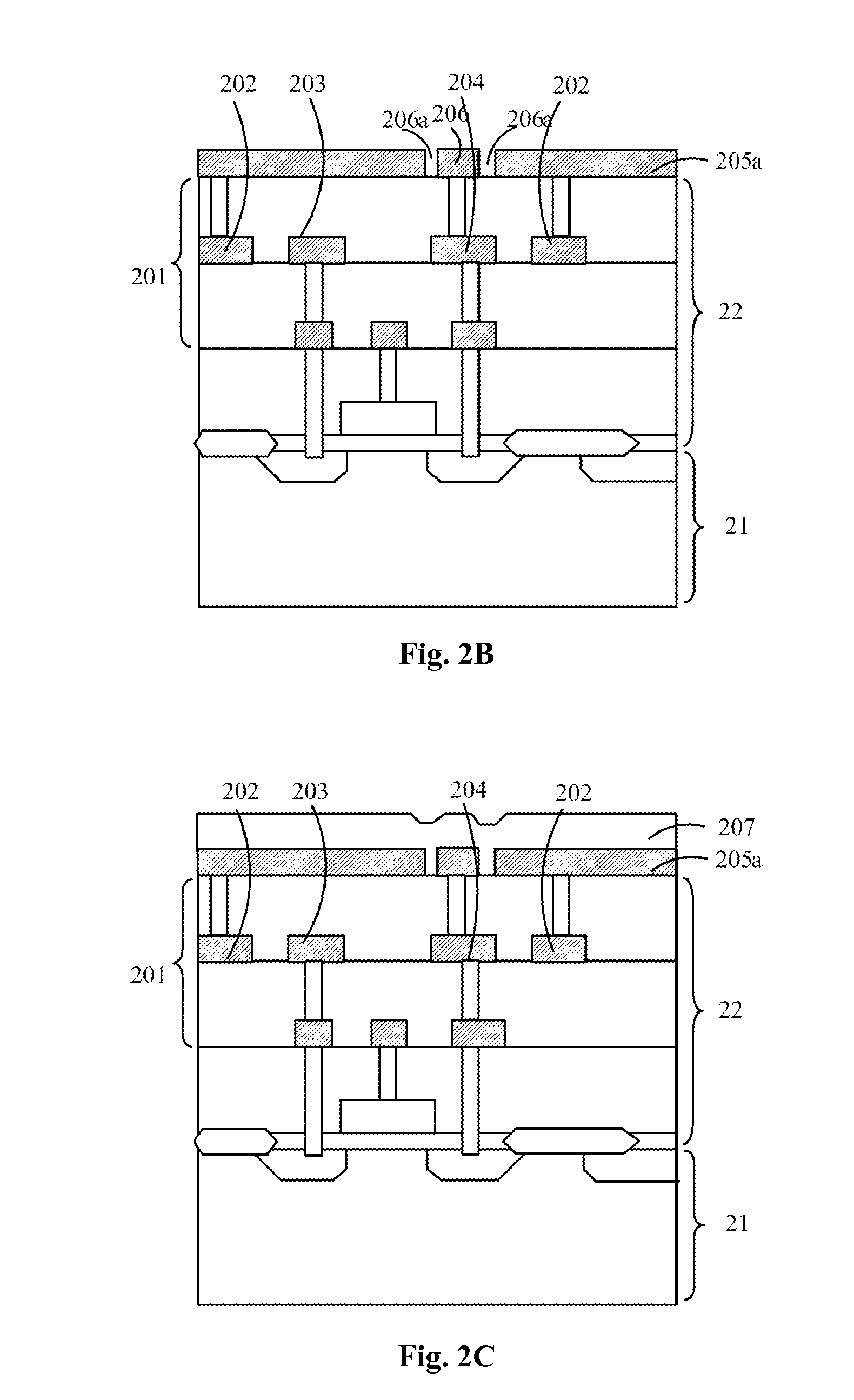
[0029]A method for forming a Liquid Crystal on Silicon (LCOS) display unit is now described, which includes: forming a pixel switch circuit layer on a silicon substrate, the pixel switch circuit layer including a Metal-Oxide-Semiconductor Field-Effect Transistor (MOSFET); forming a light shielding layer on the pixel switch circuit layer; forming an insulation layer on the light shielding layer; forming a micromirror layer on the insulation layer; wherein the micromirror layer, the insulation layer and the light shielding layer constitute a capacitor, the micromirror layer is electrically connected with a source of the MOSFET, and the light shielding layer is grounded.

[0030]FIGS. 2A to 2J illustrating a method for forming an LCOS display unit according to an embodiment of ...


PUM


Abstract

An embodiment of the present invention discloses a Liquid Crystal on Silicon (LCOS) display unit, in which a Metal-Insulator-Metal (MIM) capacitor consisting of a micromirror layer, a insulation layer and a light shielding layer is formed by grounding the light shielding layer on a pixel switch circuit layer. Therefore the pixel switch circuit and the capacitor are in vertical distribution, that is, the switch circuit and the capacitor both have an allowable design area of the size of one pixel. Another embodiment of the present invention provides a method for forming a Liquid Crystal on Silicon (LCOS) display unit.

Description

FIELD OF THE PRESENT INVENTION[0001]The present invention relates to semiconductors, and more particularly, to a Liquid Crystal on Silicon (LCOS) display unit and a method for forming the same.BACKGROUND OF THE PRESENT INVENTION[0002]In recent years, many new technologies related to Liquid Crystal Displays (LCD) have come forth, and among others, Liquid Crystal on Silicon (LCOS) is a hot technology. LCOS relates to a new reflective micro LCD projection technology. To form an LCOS structure, transistors are grown on a silicon substrate; a drive panel (also referred to as Complementary Metal-Oxide-Semiconductor-LCD (CMOS-LCD)) is fabricated using a semiconductor process; the transistors are flattened by polishing technology and plated with aluminum to act as micro mirrors; thus a Complementary Metal-Oxide-Semiconductor (CMOS) substrate is formed; then the CMOS substrate is jointed with an upper glass substrate having transparent electrodes, and liquid crystal is injected into the stru...

Claims


Application Information

Patent Timeline
IPC IPC(8): G02F1/136H01L21/77
CPCG02F1/133553G02F1/136209G02F1/136277H01L29/78654H01L27/1214H01L27/13H01L29/78633H01L27/12
Inventor HUANG, HERB HEPU, XIANYONGMAO, JIANHONGCHEN, YIQUNFU, JINGHONG, ZHONGSHANXIANG, YANGHUI
Owner SEMICON MFG INT (SHANGHAI) CORP
Why Eureka
Try Eureka