Coating and developing system, coating and developing method and storage medium

Active Publication Date: 2008-06-05
TOKYO ELECTRON LTD
View PDF8 Cites 25 Cited by
  • Summary
  • Abstract
  • Description
  • Claims
  • Application Information

AI Technical Summary

Benefits of technology

[0037]According to the present invention, the coating film forming unit block is provided with the buffer module. The difference in processing rate between the coating film forming unit block and the exposure system can be absorbed by holding the substrate processed by the coating film forming unit block by the buffer module until the exposure system becomes ready to process the substrate when the processing rate at which the coating film forming unit block processes substrates is higher than that at which the exposure system processes substrates. When the buffer module is installed in the coating film forming unit block, load on the interface block is lower than that loaded on the interface block when the buffer module is installed in the interface block. Consequently, the number of the interface arms can be reduced and the manufacturing cost can be reduced. Since the interface block needs a reduced number of interface arms, the footprint of the interface block is small.
[0038]The buffer mo

Problems solved by technology

However, when the large buffer 16 having a large capacity, and the two carrying arms 18A and 18B are installed in the interface block 1C, the interface block 1C needs a large footprint, and the use of the two carrying arms 18A and 18B increases the manufacturing cost and the op

Method used


Image

  • Coating and developing system, coating and developing method and storage medium
  • Coating and developing system, coating and developing method and storage medium
  • Coating and developing system, coating and developing method and storage medium

Examples


Embodiment Construction

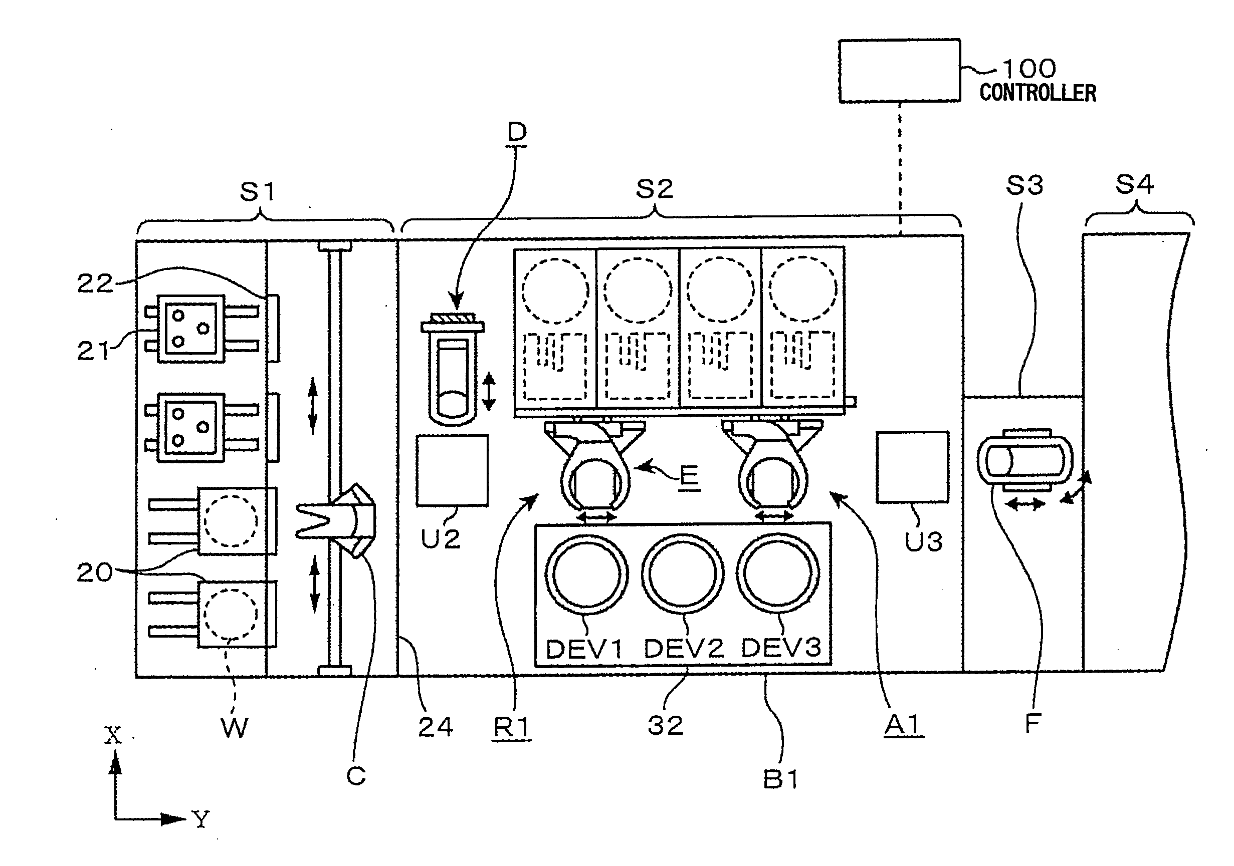
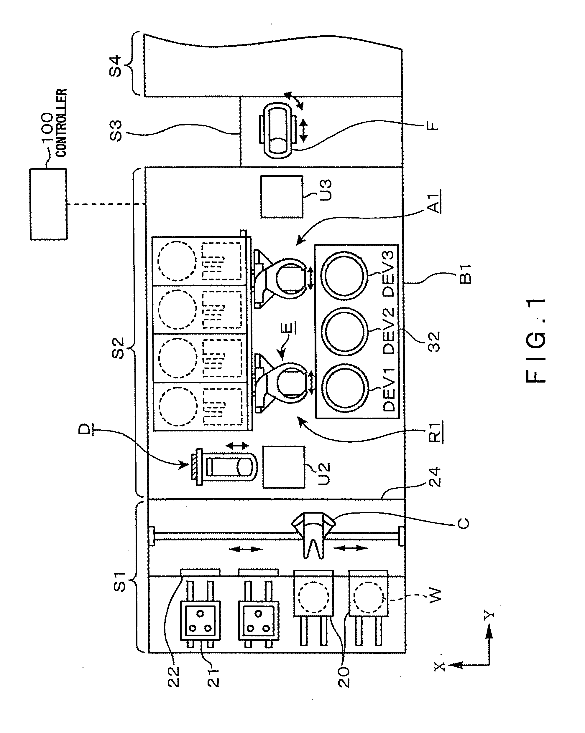
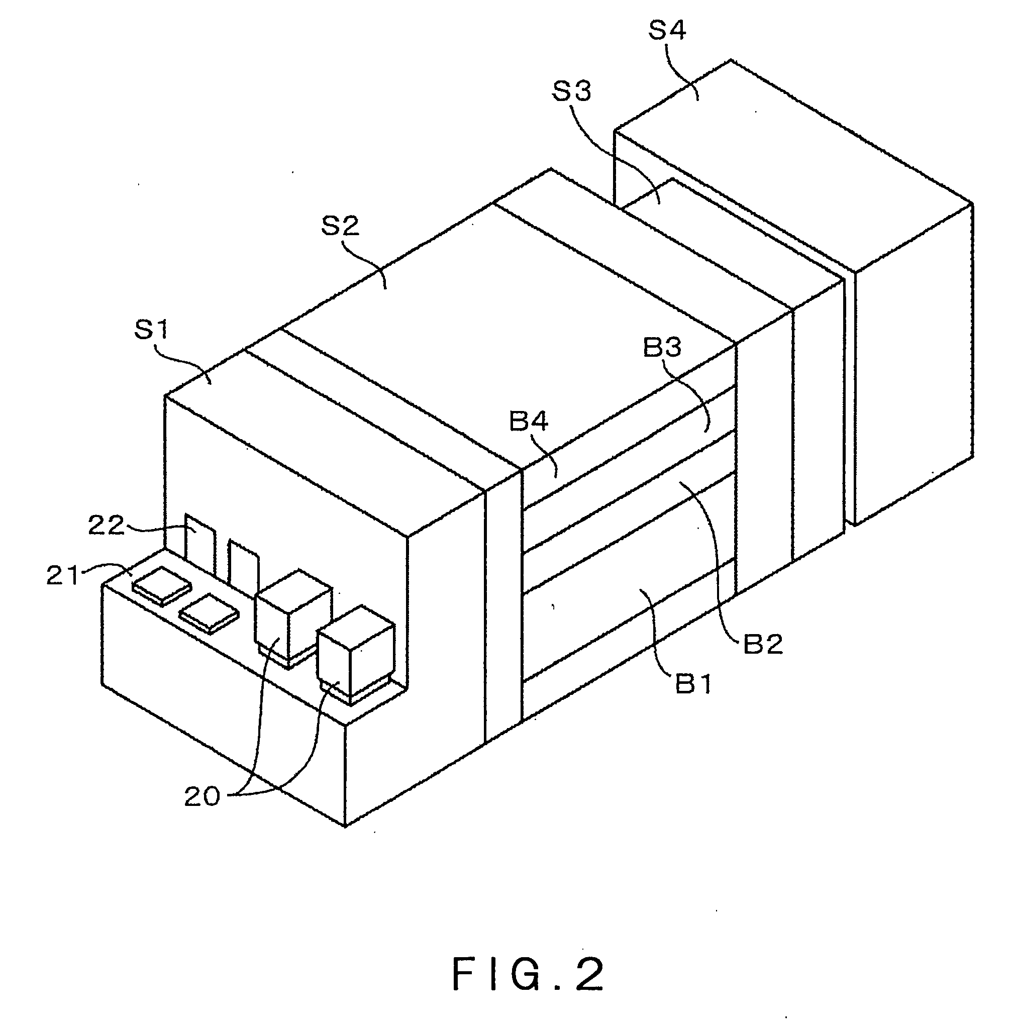
[0054]A resist pattern forming system in a preferred embodiment of a coating and developing system according to the present invention will be described with reference to the accompanying drawings. FIG. 1, FIG. 2 and FIG. 3 are a plan view, a perspective view and a schematic sectional side elevation, respectively, of the resist pattern forming system. The resist pattern forming system has carrier block S1 for receiving and sending out carriers 20 each containing, for example, thirteen wafers W, namely, substrates, in an airtight fashion, a processing block S2 formed by stacking up a plurality of unit blocks, for example, four unit blocks B1 to B4, an interface block S3, and an exposure system S4.

[0055]The carrier block S1 is provided with carrier tables 21 on which carriers 20 are supported, a wall disposed behind the carrier tables 21 and provided with closable openings 22, and a transfer arm C for taking out the wafers W from the carrier 20 through the closable opening 22. The tran...


PUM


Abstract

A buffer module is installed in a coating film forming unit block of a coating and developing system to reduce the number of interface arms needed by an interface block, and the manufacturing cost and footprint of the coating and developing system. For example, buffer modules BF31 to BF34 capable of holding a number of wafers W greater by one than the number of coating modules COT1 to COT3 of a COT layer B3 is installed in the COT layer B3, In the COT layer B3, a wafer W is carried along a carrying route passing a temperature control module CPL3, COT1 to COT3, a heating and cooling module LHP3, and the buffer modules BF31 to BF34. A main arm A3 carries wafers W such that the number of wafers W placed in the modules on the downstream side of the CPL3 is greater by one than the number of modules between the CPL3 and the buffer module when a processing rate at which an exposure system processes wafers W is lower that at which the COT layer B3 processes wafers W.

Description

BACKGROUND OF THE INVENTION[0001]1. Field of the Invention[0002]The present invention relates to a coating and developing system for coating a substrate, such as a semiconductor wafer or an LCD substrate, namely, a glass substrate for a liquid crystal display, with a resist solution by a coating process and processing the substrate by a developing process after exposure, a coating and developing method to be carried out by the coating and developing system, and a storage medium.[0003]2. Description of the Related Art[0004]A manufacturing process for manufacturing a semiconductor device or an LCD substrate forms a resist patter on a substrate by photolithography. Photolithography includes a series of steps of coating a surface of a substrate, such as a semiconductor wafer (hereinafter, referred to as “wafer”) with a resist film by applying a resist solution to the surface, exposing the resist film to light through a photomask, and processing the exposed resist film by a developing pr...

Claims


Application Information

Patent Timeline
IPC IPC(8): G03B27/42G03B27/32B05C11/08H01L21/027H01L21/677
CPCG03F7/3021H01L21/6723H01L21/67225H01L21/67196G03F7/70875H01L21/67098H01L21/67248
Inventor HAYASHIDA, YASUSHIHARA, YOSHITAKA
Owner TOKYO ELECTRON LTD
Why Eureka
Try Eureka