Specimen kit and fabricating method thereof
- Summary
- Abstract
- Description
- Claims
- Application Information
AI Technical Summary
Benefits of technology
Problems solved by technology
Method used
Image
Examples
first embodiment
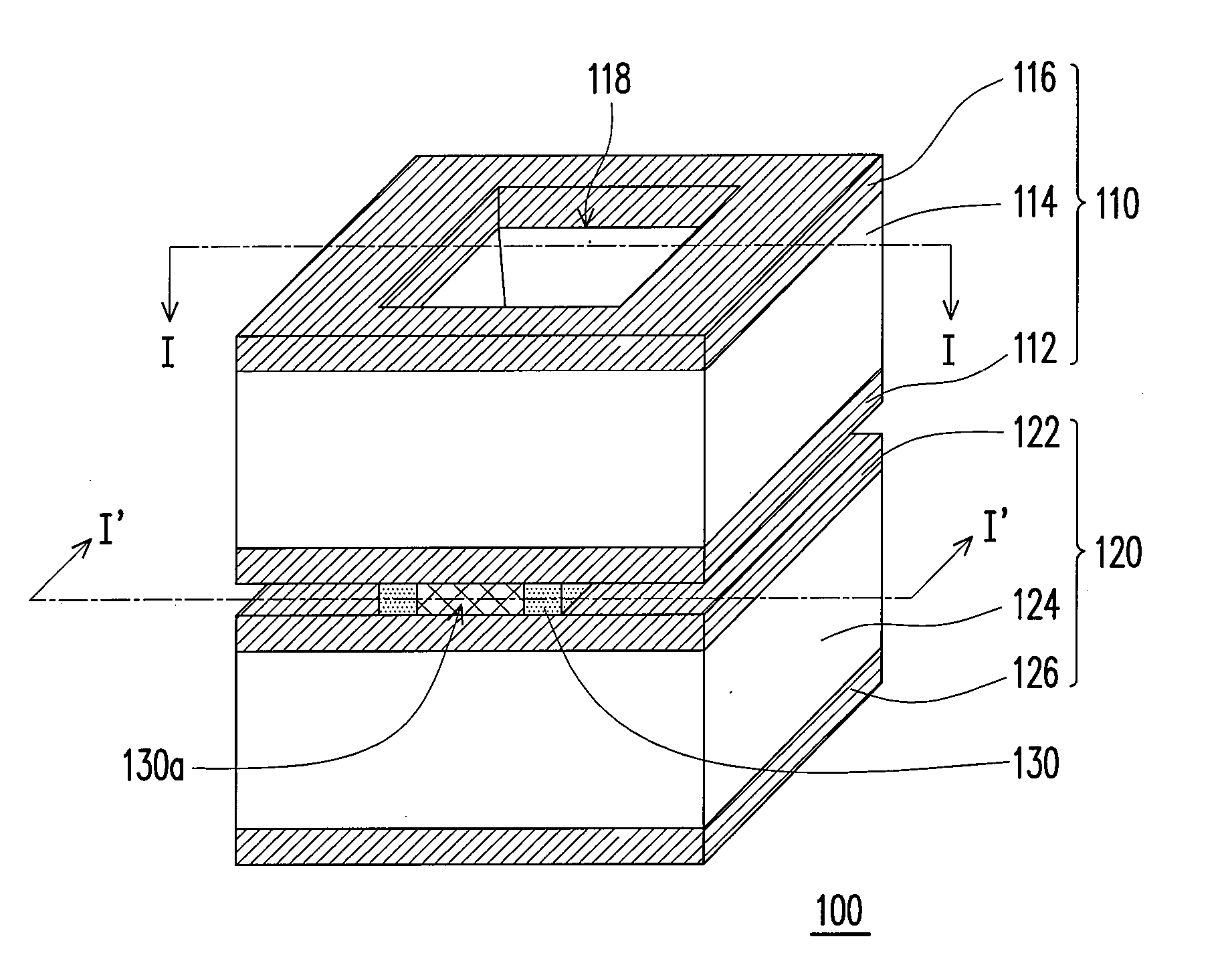
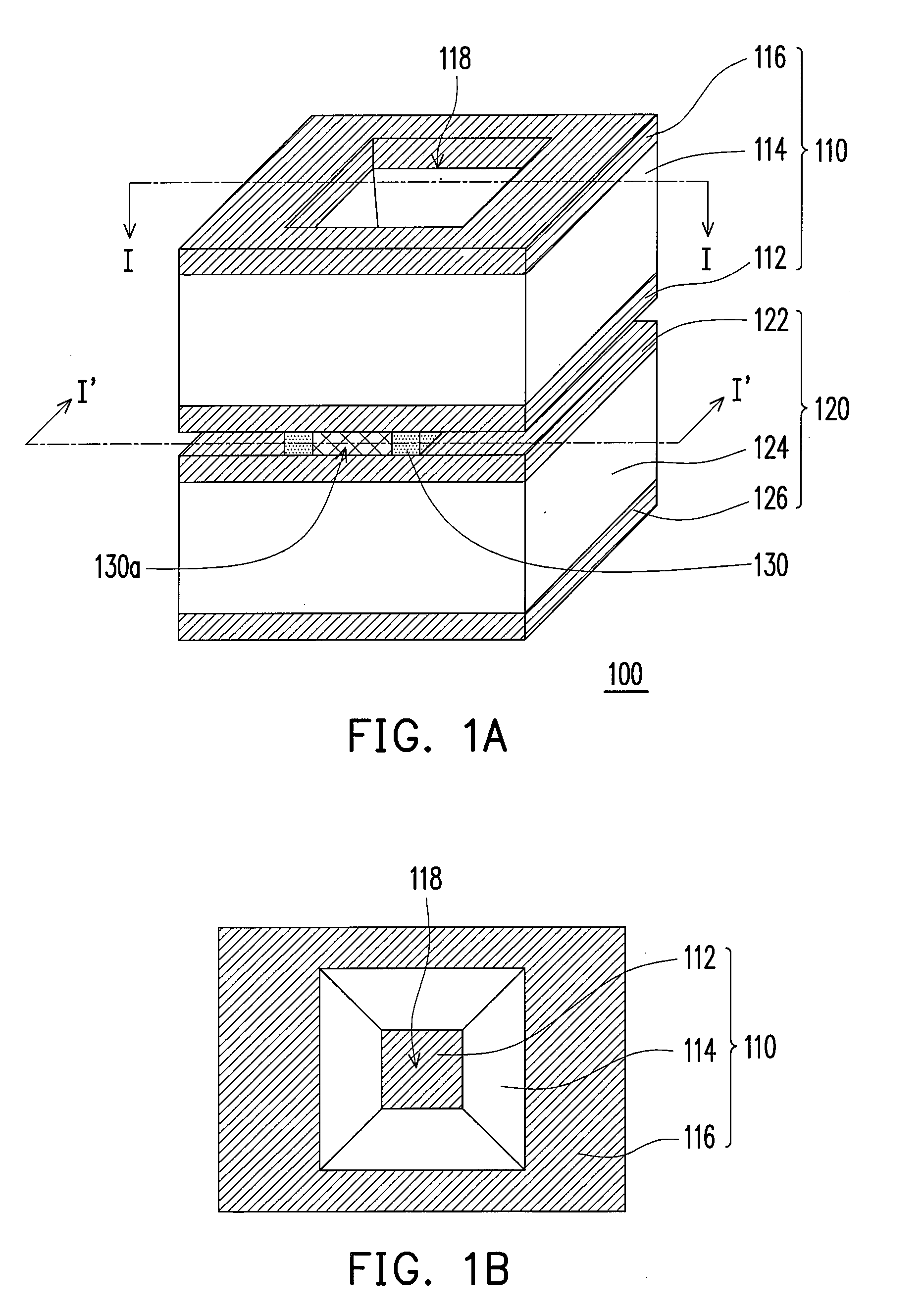
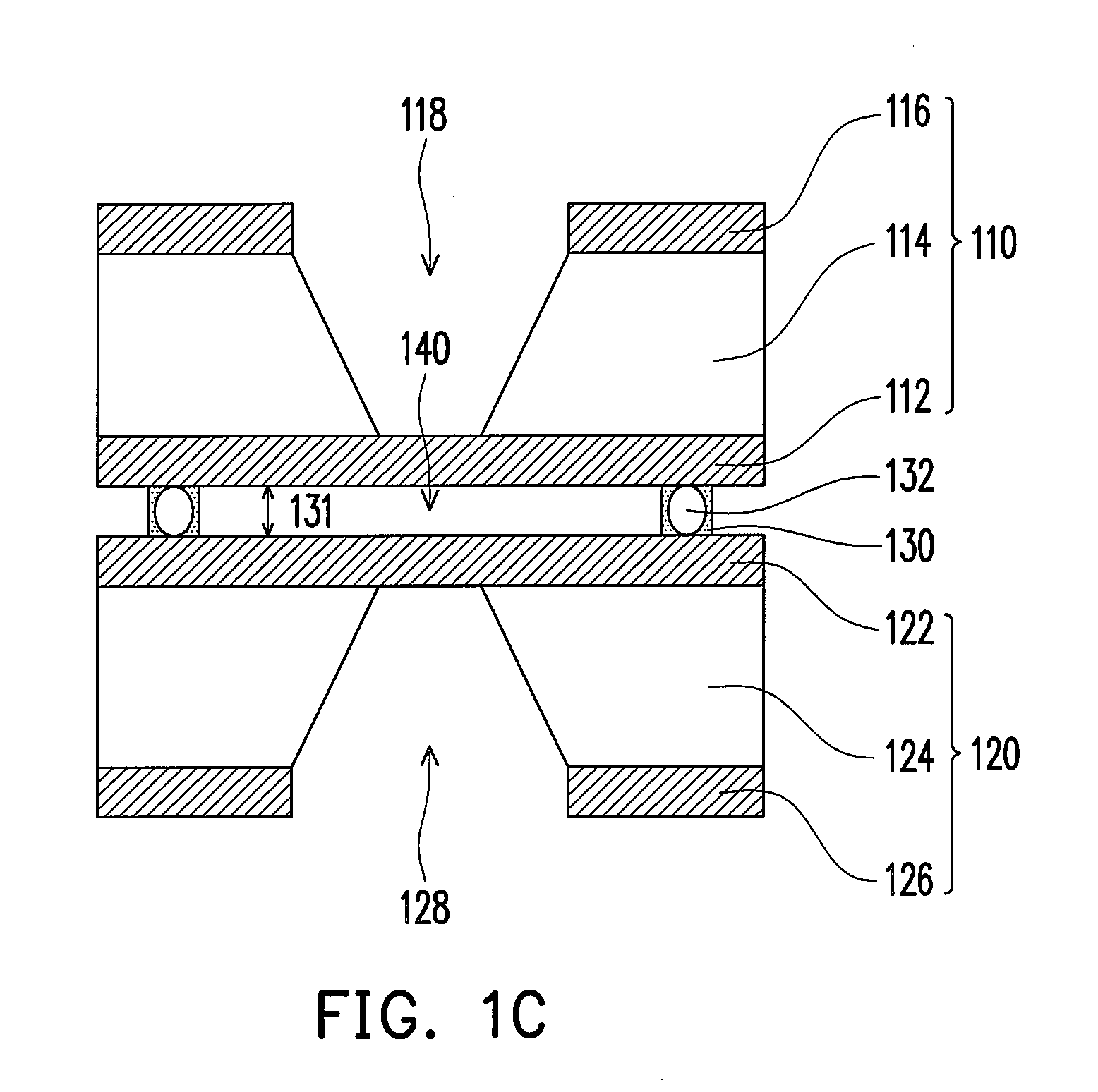
[0039]Reference is made to FIGS. 1A, 1B and 1C, which are simplified perspective, top and cross-sectional views of a specimen kit 100 according to this invention. The specimen kit 100 includes two substrates 110 and 120 and a sealant 130. The substrate 110 and 120 are disposed opposite to each other with an interval 131 between them. The interval 131 is within the range of 10 nm to 20 μm, preferably 0.1 μm to 10 μm. The sealant 130 is disposed between the substrates 110 and 120 for sealing the space between the fringes of the substrates 110 and 120.
[0040]The substrate 110 includes a support material 114 with two films 112 and 116 formed on both sides thereof. The substrate 120 includes a support material 124 with two films 122 and 126 formed on both sides thereof. The support material 114 or 124 is, for example, a semiconductor layer having been processed by single- or double-surface polishing, or a metal oxide layer, wherein the semiconductor might be silicon, silicon oxide, silico...
second embodiment
[0044]In the second embodiment, as shown in FIGS. 1D and 1D-1, the specimen kit could further include at least one micro-channel optionally. The micro-channels 119 and 129 are respectively disposed in the opposite sides of the observation windows 118 and 128, for example. That is, the micro-channel 119 or 129 encroaches the film 112 or 122 and the support material 114 or 124 thereunder. More specifically, the micro-channels 119 and 129 are surrounded by the sealant 130, so that the micro-channels 119 and 129 are located within the enclosed specimen cell 140. Each of the micro-channels 119 and 129 has a width within the range of 1 μm to 900 μm, preferably 10 μm to 500 μm, a length within the range of 1 μm to 900 μm, preferably 10 μm to 500 μm, and a depth within the range of 1 μm to 500 μm, preferably 10 μm to 250 μm.
[0045]Each of the micro-channels 119 and 129 may include separated bar-like patterns, separated arc patterns, separated half rectangular patterns or any other separated ...
PUM
| Property | Measurement | Unit |
|---|---|---|
| Thickness | aaaaa | aaaaa |
| Thickness | aaaaa | aaaaa |
| Length | aaaaa | aaaaa |
Abstract
Description
Claims
Application Information


