Packaging of Micro Devices

a micro-device and packaging technology, applied in the field of structure packaging, can solve the problems of high temperature in the process, unprotected movable components of mems devices are unlikely to survive standard packaging steps, and the cost and complexity of packaging, and achieve the effect of reducing the height of the channel

Inactive Publication Date: 2008-06-19
UNIV COLLEGE CORK NAT UNIV OF IRELAND CORK
View PDF7 Cites 17 Cited by
  • Summary
  • Abstract
  • Description
  • Claims
  • Application Information

AI Technical Summary

Benefits of technology

[0039]In one embodiment, the method comprises the further step of depositing a pad of material on the substrate under the location of at least one bridge to reduce channel height.

Problems solved by technology

A major barrier to the commercialisation of these devices is the cost and complexity of packaging.
Unlike IC's, the unprotected movable component of a MEMS device is unlikely to survive standard packaging steps such as wafer dicing, assembly, wire bonding, and encapsulation processes.
However, there are a number of problems associated with these techniques—Many bonding processes require high temperatures in order to achieve a good seal.
High temperature levels are not compatible with many process materials or MEMS structures—high temperatures may cause thermal mismatch and result in device bowing or distortion.Many methods of packaging these components also require specialist equipment or techniques that may not be commonly found within a conventional IC foundry or process.Some techniques require separate encapsulation of each individual device, a process that is expensive and time-consuming.Most wafer-to-wafer bonding or capping schemes require large areas of ‘dead’ wafer space where the bond is to be formed.
This is a very real cost in terms of the number of devices per wafer that can be fabricated.Outgassing from organic compounds using during the wafer-to-wafer bonding process may affect the hermeticity of the package cavity and have a detrimental effect on device performance.
There are several problems with this approach.
In particular, sealing material may be deposited through the etch holes and this may affect the operation of the device.
Furthermore, because of the aspect ratio of these etch holes, they may be difficult to seal in the first place.
However, the high temperatures and aggressive liquid etchants used in the fabrication process mean that this technique is unsuitable for the packaging of many metallic devices.
A problem with this approach is the height of the holes that remain between the encapsulation layer pillars.
It follows that in order to seal these high channels, a very thick sealing layer is needed, which may cause problems, in particular:thick sealing layers of silicon oxide or similar are prone to cracking.stress mismatch may occur between the thick sealing layer and the thinner encapsulation shell, causing delamination or cracking of the encapsulation layer.standard processing methods may be unable to pattern such a thick layer.the height of the channel means that it is far easier for sealing material to enter the cavity via the etch channels before closure of the channel occurs.

Method used


Image

  • Packaging of Micro Devices
  • Packaging of Micro Devices
  • Packaging of Micro Devices

Examples


Embodiment Construction

Brief Description of the Drawings

[0046]The invention will be more clearly understood from the following description of some embodiments thereof, given by way of example only with reference to the accompanying drawings in which:—

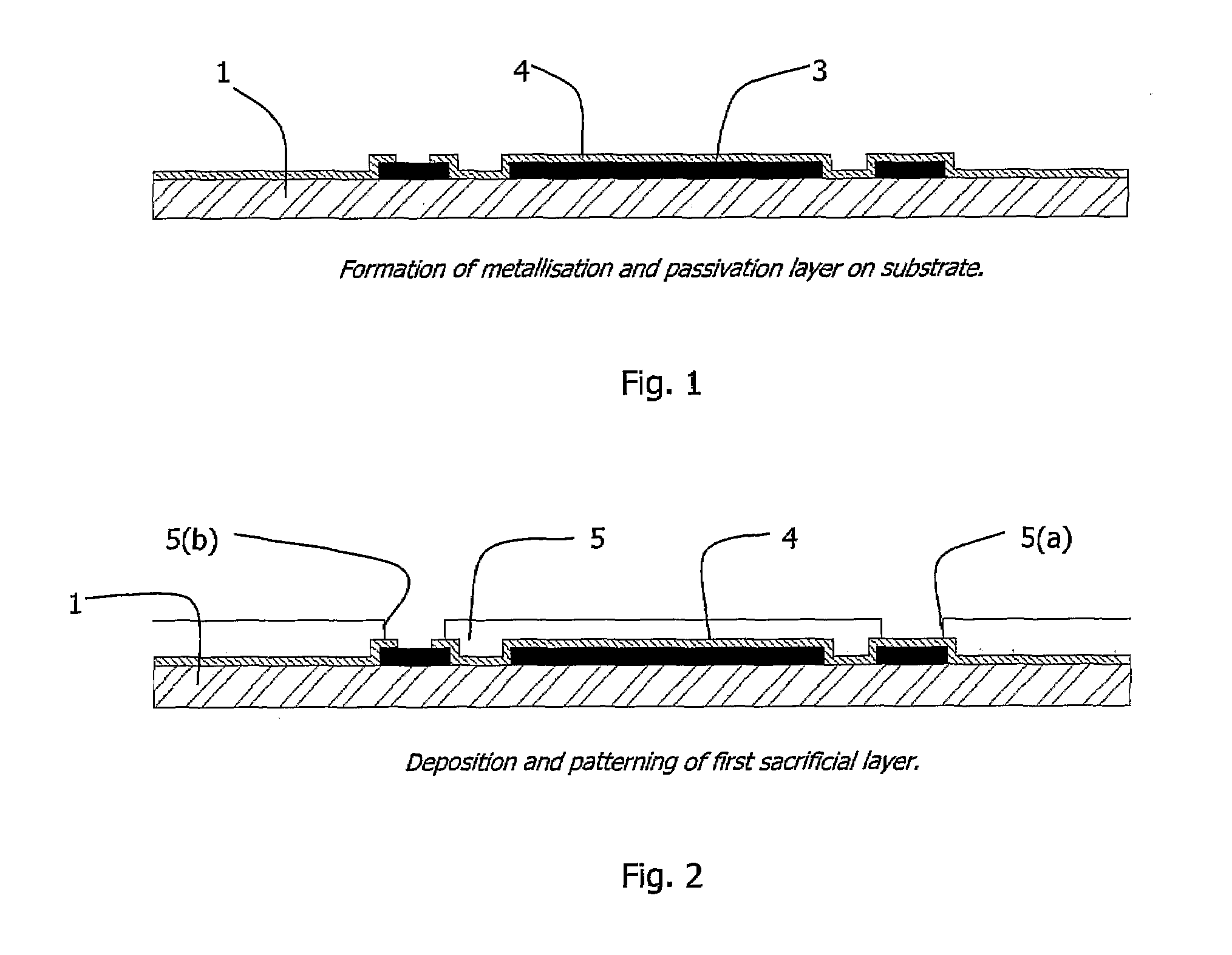
[0047]FIGS. 1 to 10 are cross-sectional diagrams showing a packaging process of the invention;

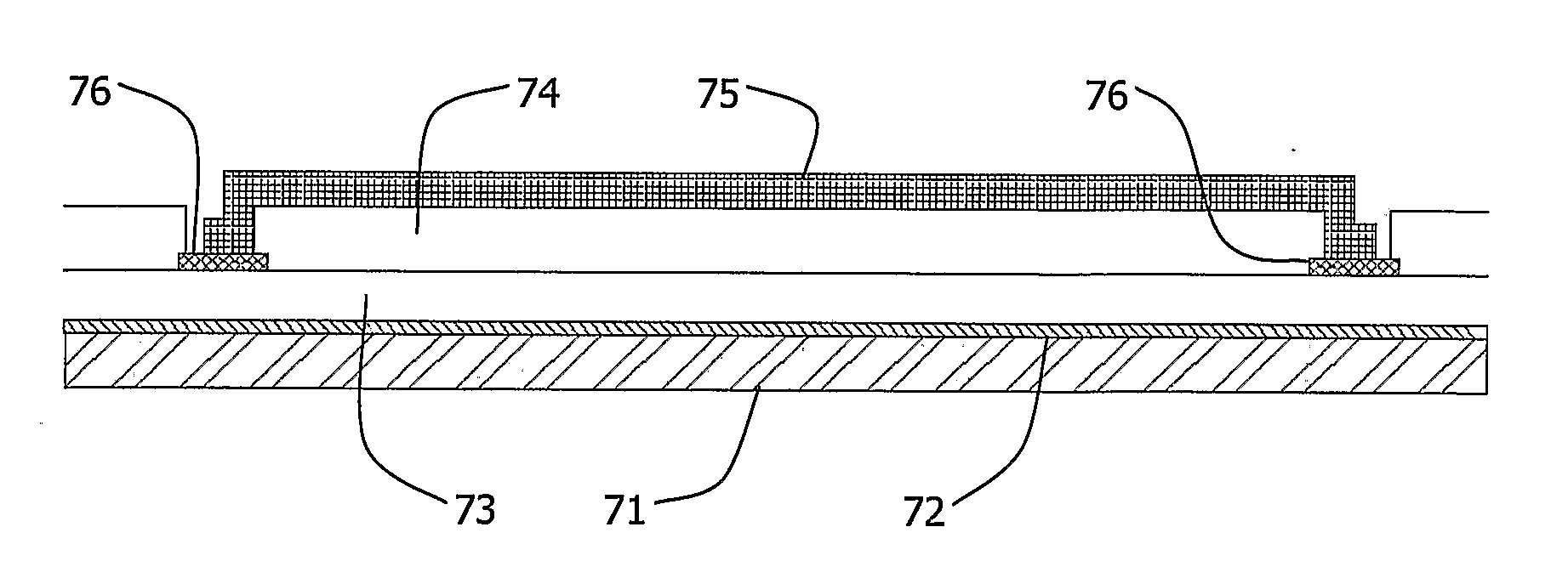
[0048]FIG. 11 is a diagram showing a final packaged device and the key to shadings used in the preceding drawings;

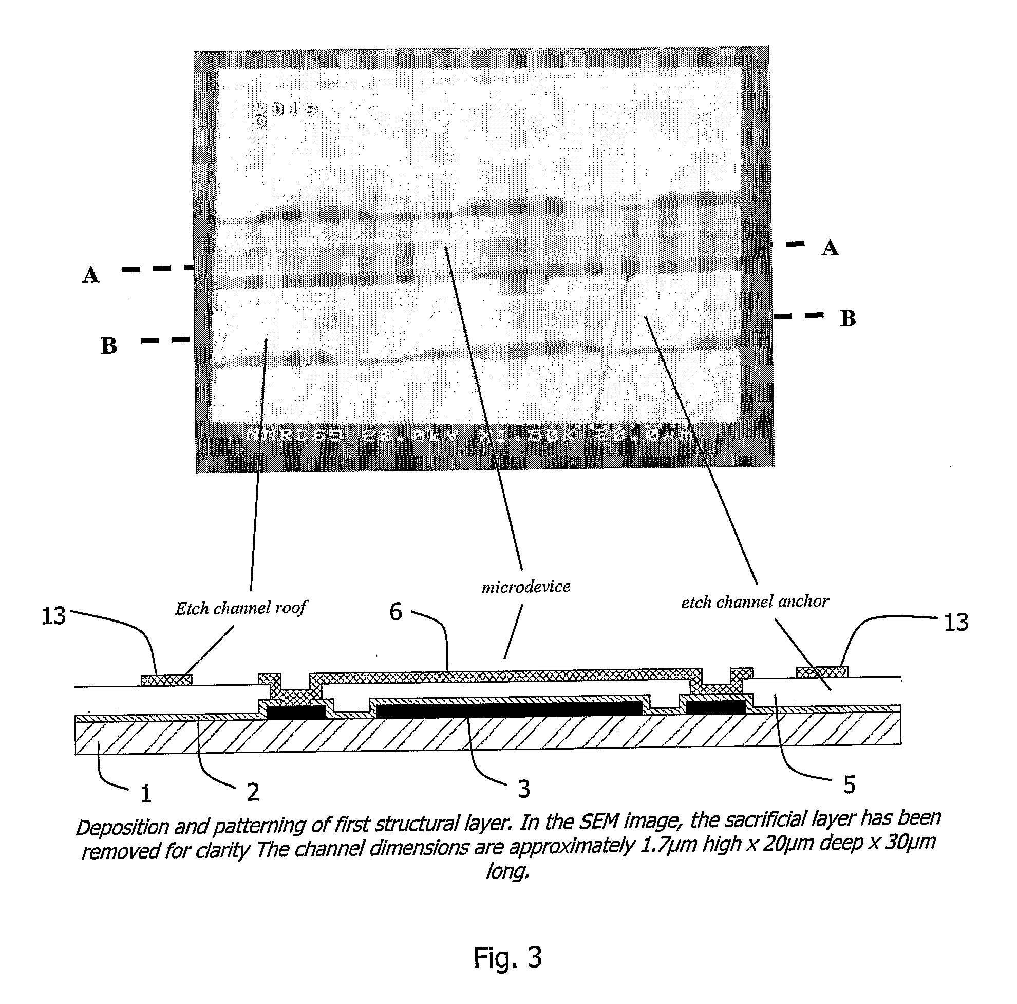
[0049]FIG. 12 is an SEM image of a fabricated and sealed micro-cavity;

[0050]FIG. 13 is a plan view photograph of a fabricated and sealed micro-cavity, illustrating the structure within;

[0051]FIG. 14 is an electromechanical result showing the performance characteristics of a packaged structure; and

[0052]FIGS. 15 and 16 are cross-sectional diagrams illustrating alternative embodiments.

DESCRIPTION OF THE EMBODIMENTS

[0053]Referring to FIG. 1, in a packaging process a silicon wafer is used as the substrate 1. However, depending on the device, the substrate mat...


PUM

PropertyMeasurementUnit
thicknessesaaaaaaaaaa
thicknessaaaaaaaaaa

Abstract

A silicon wafer is used as a substrate (1). A thin layer of metal is deposited and etched to form device metallisation (3), including electrodes and bondpads. A passivation layer (4) of silicon nitride is patterned to open access points to the metal. A lower sacrificial layer (5) is formed from polyimide and is patterned (at 5(a) and 5(b)) to open anchor regions for a device and for bridges that will define lateral etch channels for package evacuation. Structural materials that form a MEMS device (6) and bridges (13) are then deposited and patterned. The bridges (13) are patterned simultaneously with the device 6 on the lower sacrificial layer (5). An upper sacrificial layer (7) is then deposited over the device (6) and the lower sacrificial layer (5) and is patterned to open anchor regions (8) for an encapsulation layer (10). Both sacrificial layers are then simultaneously removed in an oxygen plasma ash through lateral etc channels (15). This step leaves a hollow and empty shell, inside which the MEMS device (6) is present. The device (6) is free to move after sacrificial layer removal and has clearance both above and below. The etch channels (15) are sealed by a sealant (40) applied over the encapsulant layer.

Description

FIELD OF THE INVENTION[0001]The invention relates to packaging of structures such as microelectromechanical systems (MEMS) devices.PRIOR ART DISCUSSION[0002]Advances in microelectromechanical systems (MEMS) have been rapid since the early 1970's, and micromachined components are now commonly found in uses such as accelerometers and low-cost medical applications. Radio-frequency components for mobile communications are also the subject of intensive research; these include switches, HF frequency filters, phase shifters, inductors, varactors and micromechanical resonators.[0003]A major barrier to the commercialisation of these devices is the cost and complexity of packaging. Unlike IC's, the unprotected movable component of a MEMS device is unlikely to survive standard packaging steps such as wafer dicing, assembly, wire bonding, and encapsulation processes. Furthermore, the final package must allow the device to move freely, yet provide protection from contaminants and rough handling....

Claims


Application Information

Patent Timeline
Patent Type & Authority Applications(United States)
IPC IPC(8): H01L21/58
CPCB81C1/00293B81C2203/0145B81C2203/0136
Inventor O'MAHONY, CONORHILL, MARTIN
Owner UNIV COLLEGE CORK NAT UNIV OF IRELAND CORK
Why Eureka
Try Eureka