
Method for Manufacturing Dielectric Thin Film Capacitor

a dielectric thin film capacitor and manufacturing method technology, applied in the direction of thin/thick film capacitors, capacitors, electrical appliances, etc., can solve the problem of increasing the leakage current between the upper electrode and the lower electrod

Inactive Publication Date: 2008-06-19
MURATA MFG CO LTD
View PDF13 Cites 26 Cited by
  • Summary
  • Abstract
  • Description
  • Claims
  • Application Information

AI Technical Summary

Benefits of technology

The present invention relates to a method for manufacturing a dielectric thin film capacitor. The method includes steps of depositing a lower electrode, a dielectric layer, and an upper electrode on a substrate in that order to form a capacitor structure. A resist pattern is then formed on the capacitor structure and parts of the structure are removed using dry etching. The resulting structure is then heated in an oxidative atmosphere to remove any remaining resist pattern. A protective layer is then formed covering at least a part of the capacitor structure. The method prevents stress concentration at the end of the capacitor structure and reduces cracks in the protective layer. The heat treatment after tapering the capacitor structure also prevents leak current and reduces resist residue. The technical effects of the invention include simplifying the manufacturing process, lowering production costs, and improving the function of the protective layer.

Problems solved by technology

Furthermore, the inventors found a problem in that leak current which flows between the upper electrode and the lower electrode is increased because electrical insulation of the end surface of the dielectric layer treated by dry etching is lowered by damage by the dry etching.

Method used


Image

  • Method for Manufacturing Dielectric Thin Film Capacitor
  • Method for Manufacturing Dielectric Thin Film Capacitor
  • Method for Manufacturing Dielectric Thin Film Capacitor

Examples


first embodiment

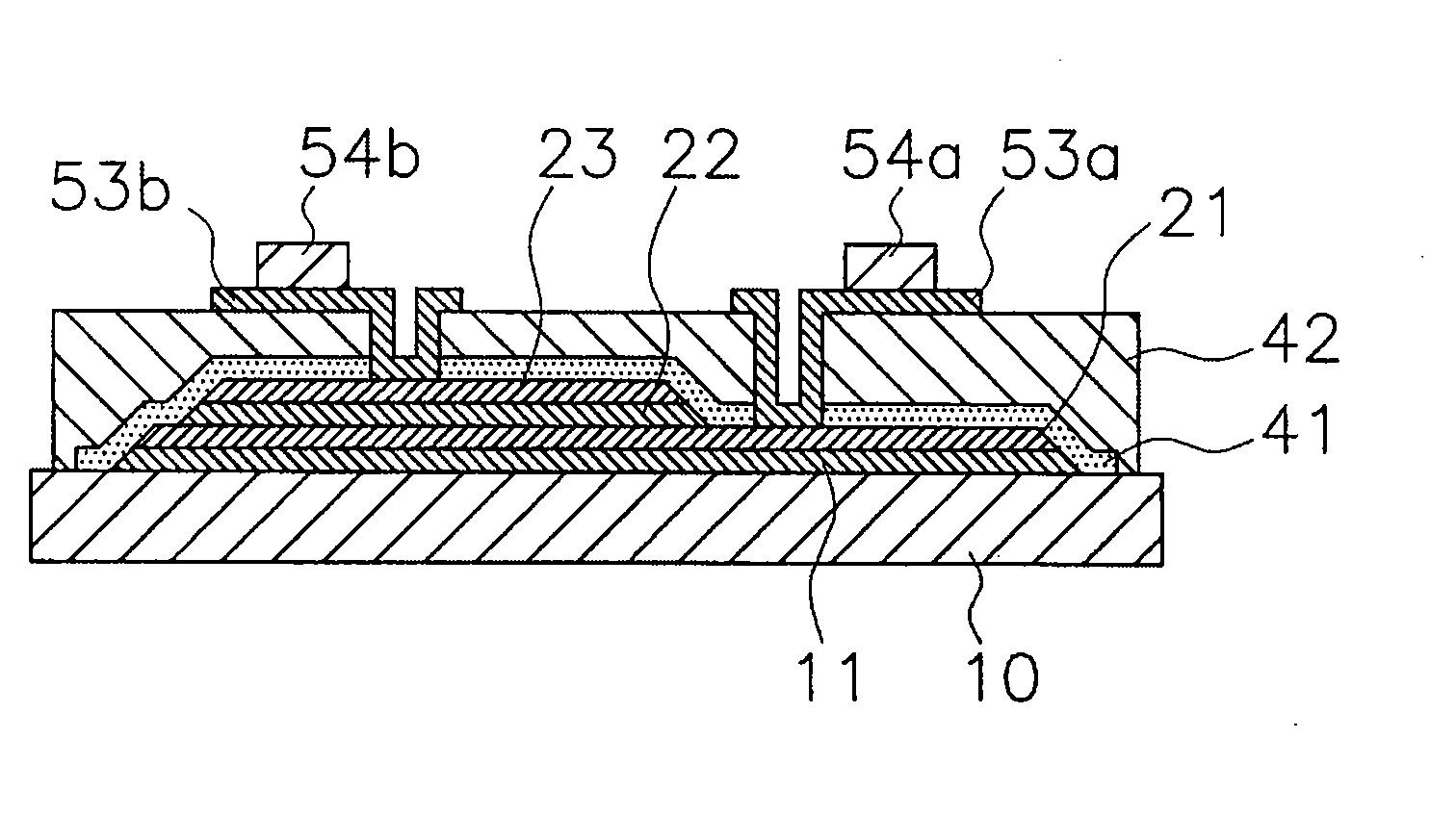
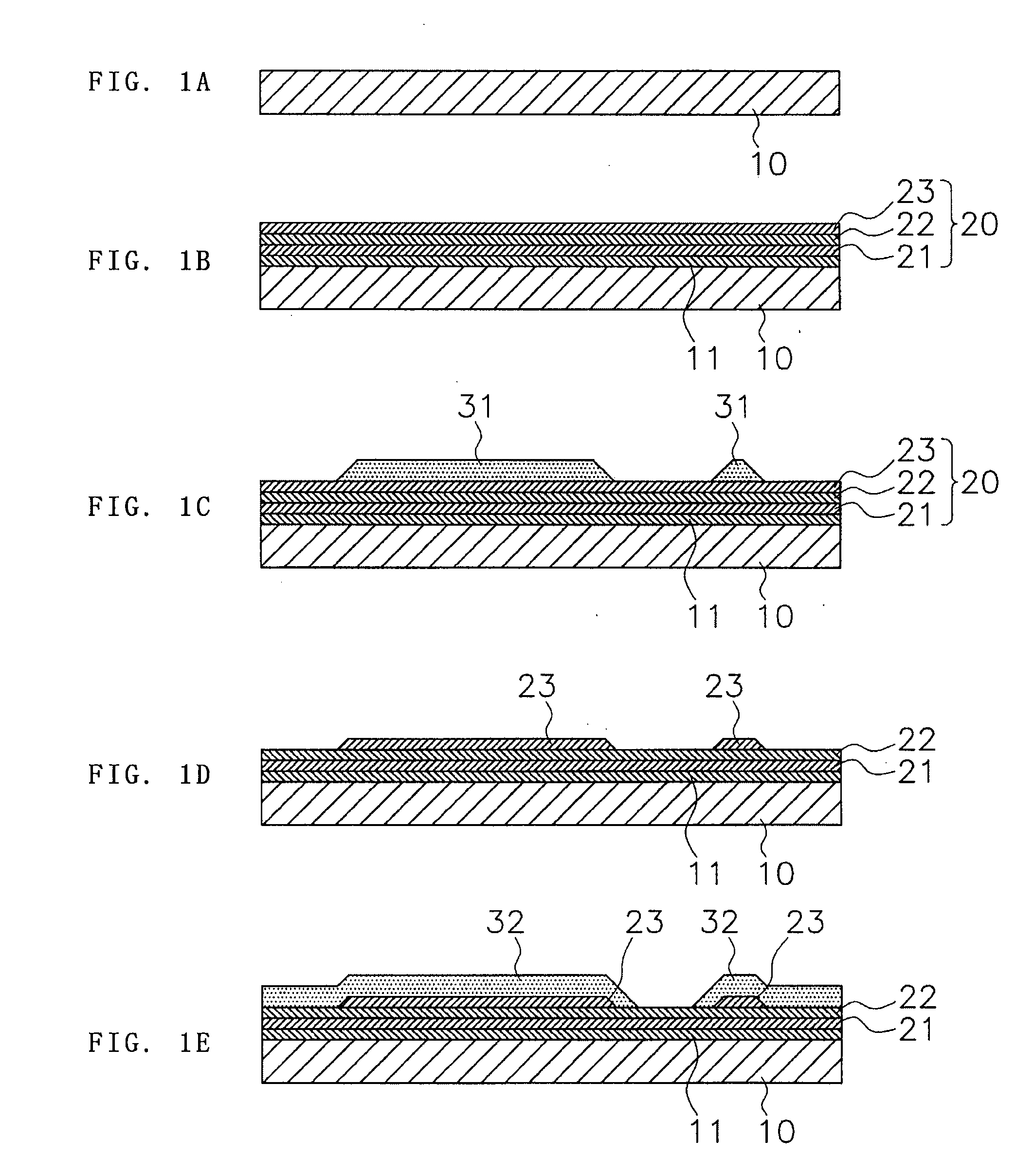
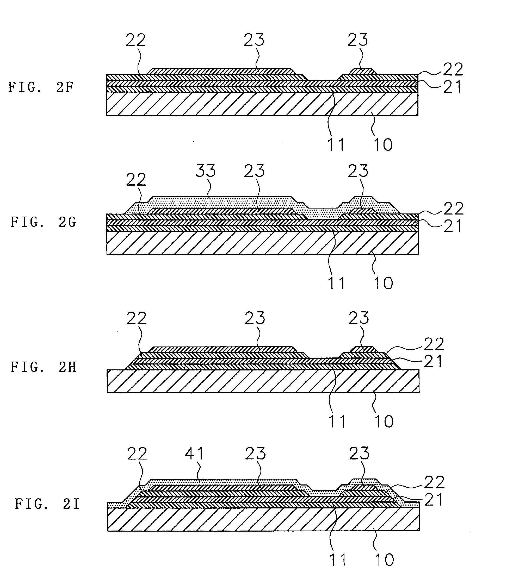
[0040]A preferred embodiment of the present invention will be described below with reference to the drawings. FIGS. 1A to 3L are cross-sectional views showing respective steps for manufacturing a dielectric thin film capacitor according to a first embodiment of the present invention.

[0041]As shown in FIG. 1A, a substrate 10 is prepared and an adhesive layer 11, a lower electrode 21, a dielectric layer 22, and an upper electrode 23 are stacked in that order on the substrate 10 as shown in FIG. 1B. A silicon substrate, a sapphire substrate, a quartz substrate, or the like can be used as the substrate 10. The adhesive layer 11 is deposited to improve the adhesion between the substrate 10 and the lower electrode 21. TiO2 or Al2O3 can be preferably used as a material of the adhesive layer 11. A layer of dielectric material having the same composition as the dielectric layer 22 can also be preferably used as the adhesive layer 11.

[0042]The lower electrode 21 and the upper electrode 23 are...

second embodiment

[0058]A preferred second embodiment of the present invention will be described below with reference to the drawings. FIGS. 4A to 6K are cross-sectional views showing respective steps for manufacturing a dielectric thin film capacitor according to a second embodiment of the present invention. Note that in FIGS. 4A to 6K, the same reference numerals will be used to denote common or similar components to those shown in FIGS. 1A to 3L, and redundant description is avoided.

[0059]As shown in FIG. 4A, a substrate 10 is provided and an adhesive layer 11, a lower electrode 21, a dielectric layer 22, and an upper electrode 23 are stacked in that order on the substrate 10 as shown in FIG. 4B. A capacitor structure 20 includes the lower electrode 21, the upper electrode 23, and the dielectric layer 22 that is held between the lower electrode 21 and the upper electrode 23 in the thickness direction.

[0060]Next, a tapered resist pattern 31 is formed on the upper electrode 23 as shown in FIG. 4C. A...

example 1

[0074]Next, EXAMPLE 1 of the present invention will be described more specifically with reference to FIGS. 1A to 3L.

[0075]As shown in FIG. 1A, a silicon substrate 10 having a thermally-oxidized film on the surface thereof (not shown) was prepared. Then, as shown in FIG. 1B, an adhesive layer 11, a lower electrode 21, a dielectric layer 22, and an upper electrode 23 were deposited in that order on the substrate 10.

[0076]The adhesive layer 11 was composed of Ba0.7Sr0.3TiO3. An MOD material solution including Ba, Sr, and Ti (at a molar ratio of 7:3:10) was prepared and applied on the substrate 10 by spin coating and then dried. Next, the resulting dried layer had a thickness of about 100 nm after rapid thermal annealing (RTA) for about 30 minutes at a temperature of about 600° C. in an oxidative atmosphere.

[0077]The lower electrode 21 was made of a Pt film having a thickness of about 200 nm that was deposited on the adhesive layer 11 by sputtering.

[0078]The dielectric layer 22 was comp...


PUM

PropertyMeasurementUnit
temperatureaaaaaaaaaa
thicknessaaaaaaaaaa
thicknessaaaaaaaaaa

Abstract

A method for manufacturing a dielectric thin film capacitor without causing cracks in a protective layer which covers a capacitor portion is provided. The method for manufacturing the dielectric thin film capacitor includes a step of forming a tapered resist pattern on a capacitor structure and a dry etching step so as to taper the end portion of the capacitor. Furthermore, a heating treatment is conducted after tapering.

Description

BACKGROUND OF THE INVENTION[0001]1. Field of the Invention[0002]The present invention relates to a method for manufacturing a dielectric thin film capacitor.[0003]2. Description of the Related Art[0004]Recently, dielectric thin film capacitors manufactured by “thin film technologies” including a metal organic decomposition (MOD) method, a sol-gel method, and a sputtering method have been studied. Such dielectric thin film capacitors have a structure in which an upper electrode and a lower electrode hold a dielectric layer formed by the thin film technology therebetween.[0005]Furthermore, in order to improve characteristics such as the reliability and the moisture resistance of the dielectric thin film capacitors, protective layers composed of organic and inorganic materials may be formed.[0006]Japanese Unexamined Patent Application Publication No. 2004-327867 discloses a thin film capacitor including electrode layers with different polarities. At least one of the electrode layers ha...

Claims


Application Information

Patent Timeline
Patent Type & Authority Applications(United States)
IPC IPC(8): H01L21/02
CPCH01G4/33H01L21/0273H01L28/40H01L21/31691H01L21/32139H01L21/31144H01L21/02197
Inventor NOMURA, MASANOBUTAKESHIMA, YUTAKAHAGI, TOSHIONAKAGAWA, NAOTOSHI
Owner MURATA MFG CO LTD
Learn More