Wiring structure of printed wiring board and method for manufacturing the same

a printing wiring board and wiring structure technology, applied in the field of wiring structure, can solve the problems of inability to realize the high density packaging of printed wiring boards freely under the present situation, failure to ensure the complete connection of a wire and a body to be wired, and the pitch of connection holes such as via holes can be reduced, so as to achieve the effect of effective fabrication of the wiring structure and reduce the pitch of connection holes

Active Publication Date: 2008-06-26
TDK CORPARATION
View PDF20 Cites 30 Cited by
  • Summary
  • Abstract
  • Description
  • Claims
  • Application Information

AI Technical Summary

Benefits of technology

[0009]With the foregoing in view, the present invention has been made. An object of the present invention is to provide a wiring structure capable of ensuring the connection between a wiring layer and a body to be wired while maintaining insulation between two adjacent wiring layers, thereby achieving pitch reduction for high density packaging; and a manufacturing process thereof.
[0022]The wiring structure and the like according to the present invention make it possible to completely connect a wiring layer and a body to be wired while maintaining insulation between two adjacent wiring layers even if the pitch of connection holes such as via-holes is decreased. A decrease in the pitch of connection holes contributes to the realization of high density packaging of a printed wiring board or the like.

Problems solved by technology

In either of the above-described manufacturing processes of wiring structure, misalignment may occur when a wiring layer is patterned.
Since a decrease in the arrangement distance of bodies to be wired needs a decrease in the via-hole pitch, high density packaging of a printed wiring board cannot be realized freely under the present situation.
There is however a fear of failing to ensure complete connection of a wire and a body to be wired when misalignment occurs therebetween.
Such a failure in connection leads to problems such as disconnection due to insufficient connection strength and an increase in the connection resistance to an undesirable level.

Method used


Image

  • Wiring structure of printed wiring board and method for manufacturing the same
  • Wiring structure of printed wiring board and method for manufacturing the same
  • Wiring structure of printed wiring board and method for manufacturing the same

Examples


Embodiment Construction

[0038]Embodiments of the present invention will next be described specifically. In all the drawings, elements having like function are identified by like reference numerals and overlapping descriptions are omitted. The positional relationship in the left-right or up-down direction is based on the positional relationship shown in these drawings unless otherwise specifically indicated. The dimensional ratio is not limited to that in the drawings. The following embodiments are shown not for limiting the invention but only for explaining the present invention. Moreover, the present invention can be modified in various ways insofar as they do not depart from the scope of the invention.

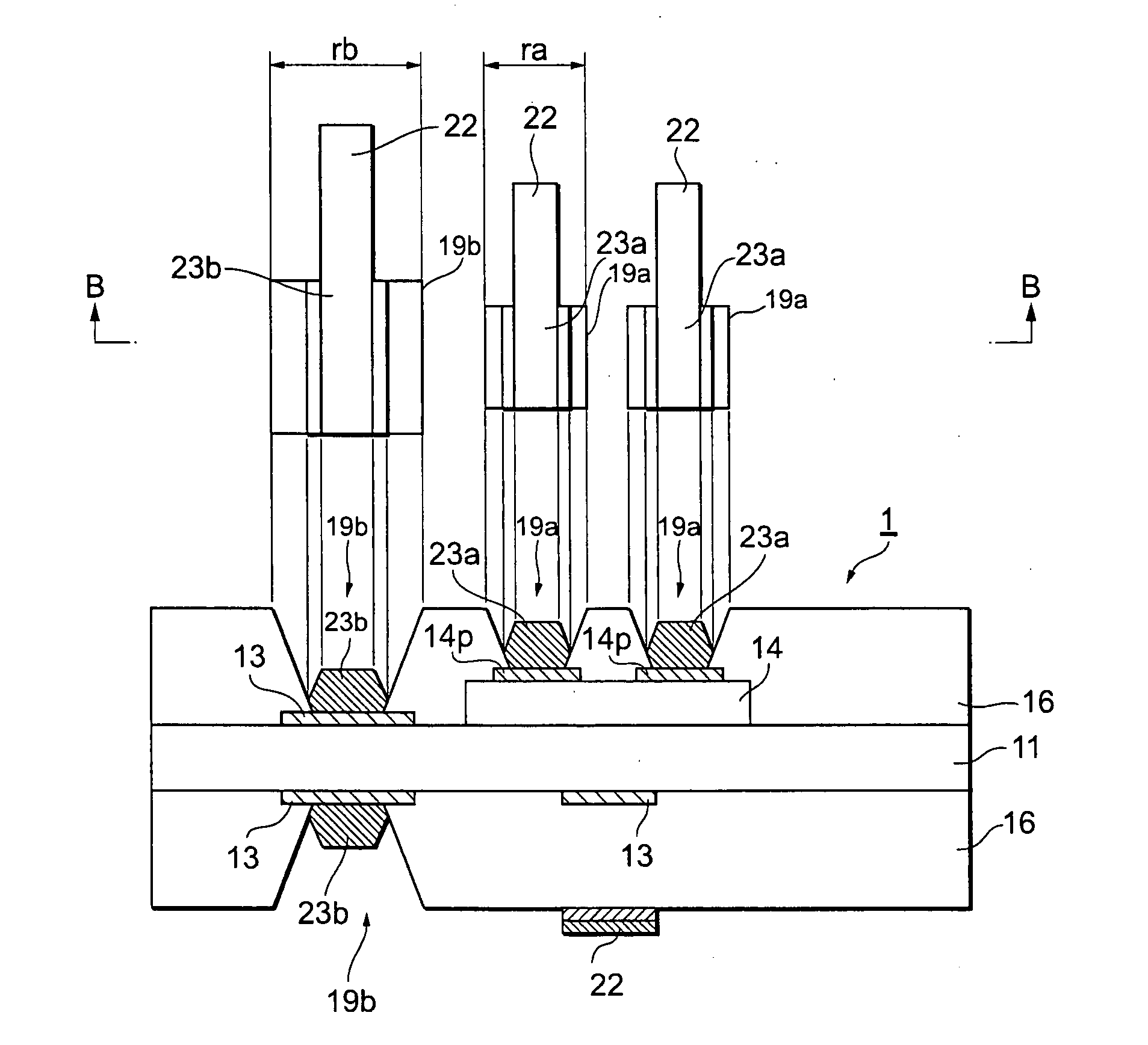
[0039]FIG. 1A is a fragmentary schematic plan view illustrating one example of semiconductor-embedded substrates having one preferred wiring structure according to the present invention; and FIG. 1B is a cross-sectional view taken along a line B-B of FIG. 1A.

[0040]In a semiconductor-embedded substrate 1 (pr...


PUM

PropertyMeasurementUnit
thicknessaaaaaaaaaa
thicknessaaaaaaaaaa
thicknessaaaaaaaaaa

Abstract

Provided is a wiring structure and the like which can completely connect a wiring layer to a body to be wired while keeping insulation between two adjacent wiring layers and realize high density packaging due to a narrowed pitch.In a semiconductor-embedded substrate, a conductive pattern is formed on both sides of a core substrate and a semiconductor device is placed in a resin layer stacked over the core substrate. The resin layer has via-holes so that the conductive pattern and a bump of the semiconductor device protrude from the resin layer. Inside the via-holes, the bump and conductive pattern are respectively connected to via-hole electrode portions whose cross-sectional area has been increased toward the bottom of the via-hole. A void is defined between the via-hole electrode portion and upper portion of the inner wall of the via-hole.

Description

BACKGROUND OF THE INVENTION[0001]The present invention relates to a wiring structure in a multilayer printed wiring board or component-embedded printed wiring board.[0002]Multilayer printed wiring boards obtained by alternately stacking an insulating layer and a wiring layer and component-embedded printed wiring boards having an insulating layer with electronic component-embedded therein are known as a high density packaging structure of electronic components such as semiconductor IC chips. In printed wiring boards having such a structure, as a method for connecting a wiring layer to a body to be wired thereto such as an underlying wiring layer or an electrode of an embedded electronic component arranged below or inside the insulating layer, a method for forming, in the insulating layer, a connection hole which is called “via-hole” to expose therefrom the body to be wired and connecting the body to be wired and the wiring layer inside the via-hole (refer to Japanese Patent Laid-Open...

Claims


Application Information

Patent Timeline
Patent Type & Authority Applications(United States)
IPC IPC(8): H05K1/16H05K3/30
CPCH01L23/5389Y10T29/4913H01L24/82H01L2224/24051H01L2224/24226H01L2224/82039H01L2924/01003H01L2924/01005H01L2924/01012H01L2924/01013H01L2924/01015H01L2924/0102H01L2924/01029H01L2924/0103H01L2924/01033H01L2924/01038H01L2924/0104H01L2924/01057H01L2924/01073H01L2924/01074H01L2924/01078H01L2924/01079H01L2924/01082H01L2924/01088H01L2924/04953H01L2924/14H01L2924/19041H01L2924/19043H01L2924/30105H05K1/185H05K3/061H05K3/243H05K3/28H05K3/4007H05K2201/0367H05K2201/09472H05K2201/09645H05K2201/10674H05K2203/054H05K2203/1152H01L2924/01006H01L2924/01019H01L2924/01024H01L2924/01037H01L2924/01047H01L2924/014H01L24/24H01L2924/181H01L2924/12042H01L2924/00H05K3/46
Inventor NAGASE, KENJIKAWABATA, KENICHI
Owner TDK CORPARATION
Why Eureka
Try Eureka