
Multilayer printed circuit board and multilayer printed circuit board manufacturing method

a printing circuit board and manufacturing method technology, applied in the direction of printed circuit aspects, printed circuit non-printed electric components association, printed circuit components, etc., can solve the problems of reducing the reliability of the ic chip, reducing the electrical resistance of the die pad, and reducing the electrical conductivity of the die pad

Inactive Publication Date: 2008-06-26
IBIDEN CO LTD
View PDF90 Cites 34 Cited by
  • Summary
  • Abstract
  • Description
  • Claims
  • Application Information

AI Technical Summary

Benefits of technology

This approach enhances the reliability and functionality of the multilayer printed circuit board by eliminating lead-related failures and resin-related issues, allowing for more precise alignment and connection, even with small die pads, and reduces the risk of resin residue and oxidation, thereby improving electrical conductivity and reducing wiring length.

Problems solved by technology

These lead members tend to be cut off and eroded, making the connection of the printed circuit board to the IC chip cut off or causing malfunctions.
However, if bubbles are contained at the time of filling the resin, then the lead members are broken, the IC pads are eroded and reliability of the IC chip is deteriorated due to the bubbles.
Further, in case of employing a thermosetting resin, it is necessary to select a thermosetting resin in view of the materials of the lead members, a solder resist and the like, thereby disadvantageously causing cost increase.

Method used


Image

  • Multilayer printed circuit board and multilayer printed circuit board manufacturing method
  • Multilayer printed circuit board and multilayer printed circuit board manufacturing method
  • Multilayer printed circuit board and multilayer printed circuit board manufacturing method

Examples


first embodiment

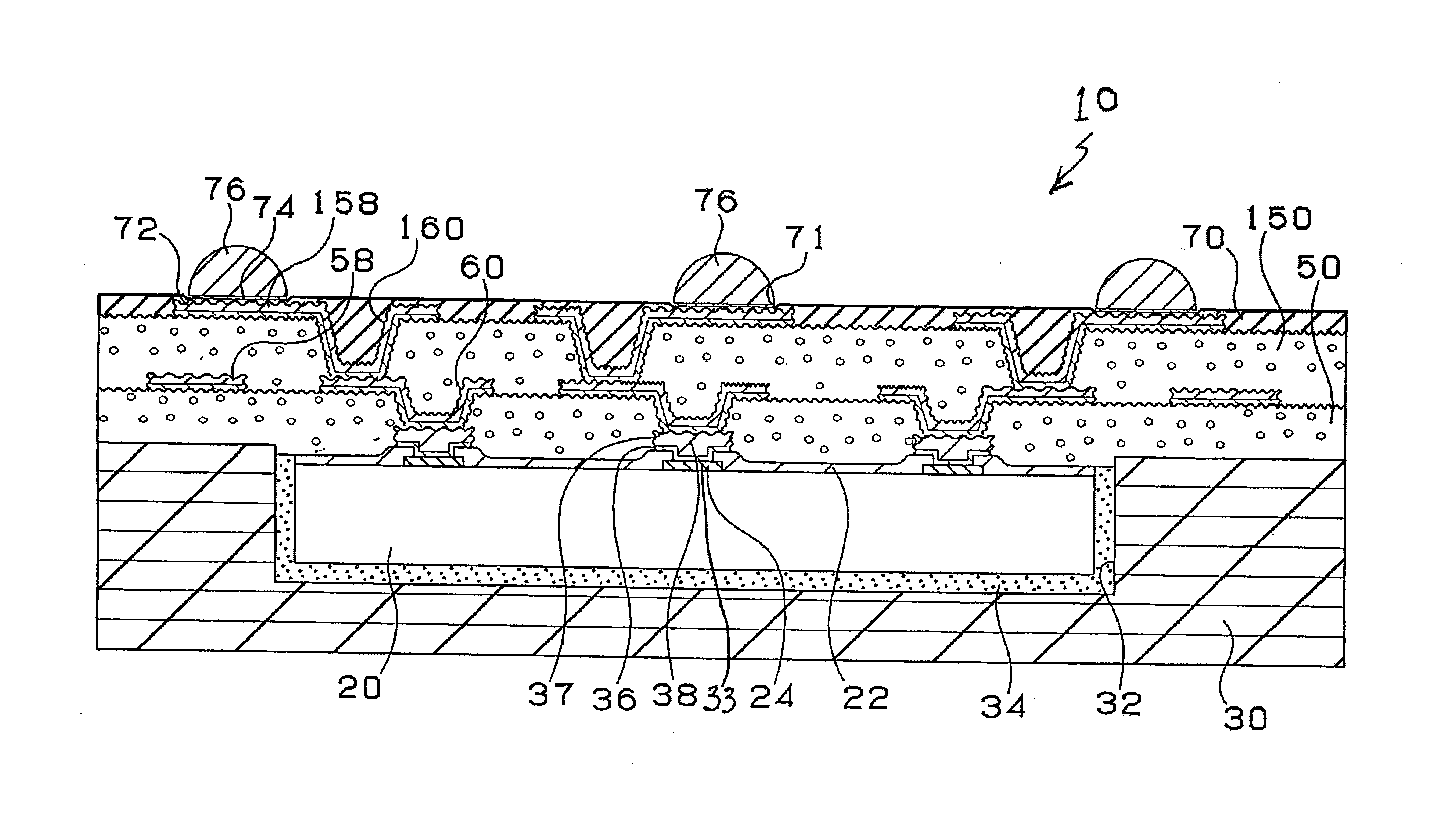
[0100]First, the constitution of a multilayer printed circuit board according to the first embodiment of the present invention will be described with reference to FIG. 6 showing the cross-sectional view of a multilayer printed circuit board 10.

[0101]As shown in FIG. 6, the multilayer printed circuit board 10 consists of a core substrate 30 containing therein an IC chip 20, an interlayer resin insulating layer 50 and an interlayer resin insulating layer 150. Via holes 60 and conductor circuits 58 are formed on the interlayer resin insulating layer 50. Via holes 160 and conductor circuits 158 are formed on the interlayer resin insulating layer 150.

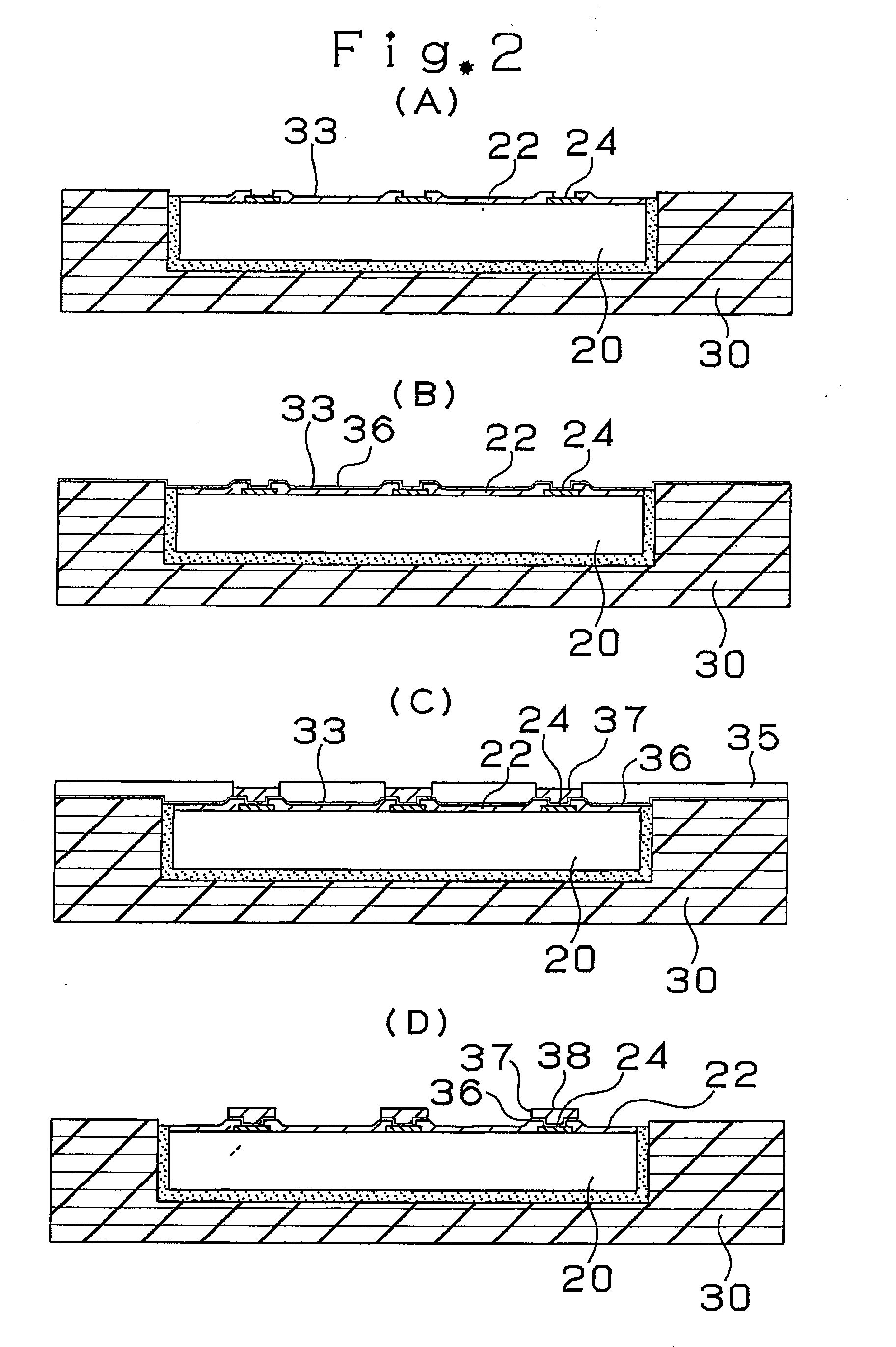
[0102]The IC chip 20 is covered with a passivation film 22 and die pads 24 each constituting an input / output terminal are provided in the openings of the passivation film 22. A transition layer 38 is formed on each die pad 24 made of aluminum. The transition layer 38 consists of three layers of the first thin film layer 33, the second thin f...

second modification

of First Embodiment

[0159]Next, description will be given to a multilayer printed circuit board according to the second modification of the first embodiment with reference to FIG. 10. In the first embodiment stated above, description has been given to a case where the BGA's are arranged. In the second modification, which is almost the same as the first embodiment, the multilayer printed circuit board is constituted in a PGA mode for establishing connection through conductive connection pins 96 as shown in FIG. 10.

third modification

of First Embodiment

[0160]Next, description will be given to a multilayer printed circuit board according to the third modification of the first embodiment with reference to FIG. 11.

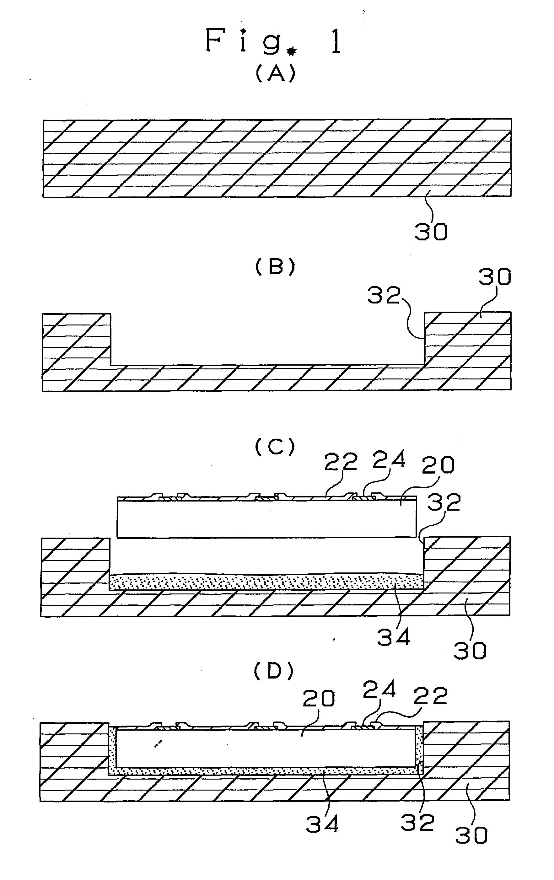
[0161]In the first embodiment stated above, the IC chip is contained in the recess 32 provided in the core substrate 30 by counter boring. In the third modification, by contrast, an IC chip 20 is contained in a through hole 32 formed in the core substrate 30. In this third modification, a heat sink can be directly attached to the rear surface side of the IC chip 20, so that it is advantageous that the IC chip 20 can be cooled efficiently.


PUM


Abstract

A multilayer printed circuit board has an IC chip 20 included in a core substrate 30 in advance and a mediate layer 38 provided on a pad 24 of the IC chip 20. Due to this, it is possible to electronically connect the IC chip to the multilayer printed circuit board without using lead members and a sealing resin. Also, by providing the mediate layer 38 made of copper on the die pad 24, it is possible to prevent resin residues on the pad 24 and to improve connection characteristics between the pad 24 and a via hole 60 and reliability.

Description

CROSS-REFERENCE TO RELATED APPLICATIONS[0001]This application is a continuation of and claims the benefit of priority under 35 U.S.C.§120 from U.S. Ser. No. 11 / 757,750, filed Jun. 4, 2007, which is a divisional of U.S. application Ser. No. 10 / 793,515 filed Mar. 4, 2004, which is a continuation of U.S. application Ser. No. 10 / 181,682, filed Jul. 17, 2002, now U.S. Pat. No. 6,909,054, issued Jun. 21, 2005, which is a National Stage, 35 USC 371, of International patent Application PCT / JP01 / 00177, filed Jan. 12, 2001, and further is based upon and claims the benefit of priority under 35 U.S.C. §119 from the prior Japanese Patent Applications No. 2000-152973, filed May 24, 2000, No. 2000-105212, filed Apr. 6, 2000, No. 2000-078206, filed Mar. 21, 2000, No. 2000-073558, filed Mar. 16, 2000, and No. 2000-049121, filed Feb. 25, 2000.TECHNICAL FIELD OF THE INVENTION[0002]The present invention relates to a buildup multilayer printed circuit board and particularly relates to a multilayer print...

Claims


Application Information

Patent Timeline
Patent Type & Authority Applications(United States)
IPC IPC(8): H05K1/18H01L21/48H01L21/60H01L23/13H01L23/498H01L23/538H01L23/544
CPCH01L21/4846H01L21/4857H01L23/13H01L23/49811H01L23/49816H01L23/49822H01L23/49827H01L23/5389H01L23/544H01L24/19H01L24/24H01L25/03H01L25/18H01L2223/54426H01L2223/54473H01L2223/5448H01L2223/54486H01L2224/04105H01L2224/16H01L2224/20H01L2224/24227H01L2224/32225H01L2224/83192H01L2224/92H01L2224/92244H01L2924/01002H01L2924/01005H01L2924/01011H01L2924/01012H01L2924/01013H01L2924/01015H01L2924/01018H01L2924/0102H01L2924/01025H01L2924/01027H01L2924/01029H01L2924/0103H01L2924/01033H01L2924/01039H01L2924/01046H01L2924/01047H01L2924/0105H01L2924/01052H01L2924/01074H01L2924/01078H01L2924/01079H01L2924/01082H01L2924/14H01L2924/15153H01L2924/1517H01L2924/15174H01L2924/15311H01L2924/15312H01L2924/1532H01L2924/18162H01L2924/30107H05K1/185H05K3/4602H05K2201/09036H05K2201/09563H05K2201/096H05K2201/09918H05K2201/10674H01L24/29H01L24/32H01L2924/01006H01L2924/01019H01L2924/01023H01L2924/01024H01L2924/01043H01L2924/014H01L24/83H01L24/18H01L2224/73267H01L2224/0401Y10T29/49165Y10T29/49133Y10T29/49128Y10T29/49155Y10T29/49126Y10T29/49147Y10T29/4913Y10T29/49144Y10T29/49156H01L2224/83H01L2224/82H01L2924/3512H01L2924/00H01L2924/12042H01L2224/45144H01L2224/12105H01L2224/16227H05K1/16
Inventor SAKAMOTO, HAJIMESUGIYAMA, TADASHIWANG, DONGDONGKARIYA, TAKASHI
Owner IBIDEN CO LTD
Learn More