
Vertical cavity surface-emitting laser and method of fabricating the same

Inactive Publication Date: 2008-06-26
SAMSUNG ELECTRONICS CO LTD
View PDF0 Cites 18 Cited by
  • Summary
  • Abstract
  • Description
  • Claims
  • Application Information

AI Technical Summary

Benefits of technology

[0012]In addition, the present invention provides a vertical cavity surface-emitting laser (VCSEL), in which in one exemplary aspect the alignment between a light output side aperture and an oxide aperture formed due to the formation of a current blocking layer can be easily implemented. The present invention includes a method of fabricating a VCSEL following steps disclosed herein below.
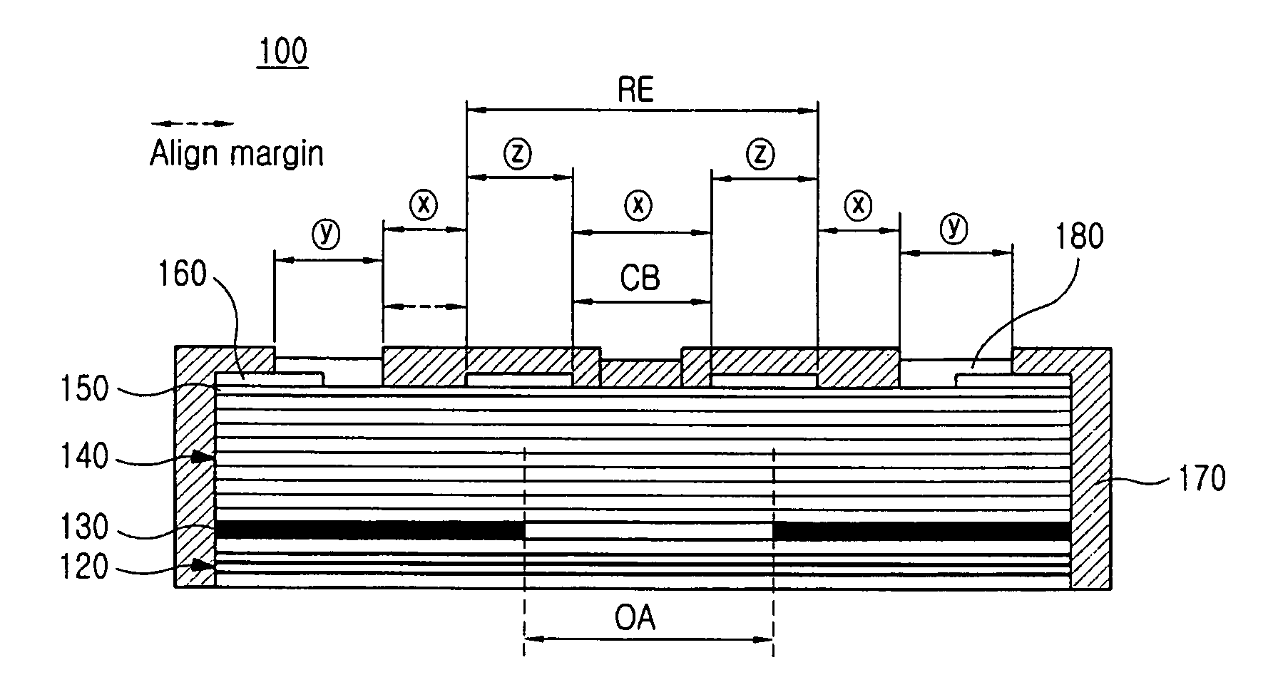
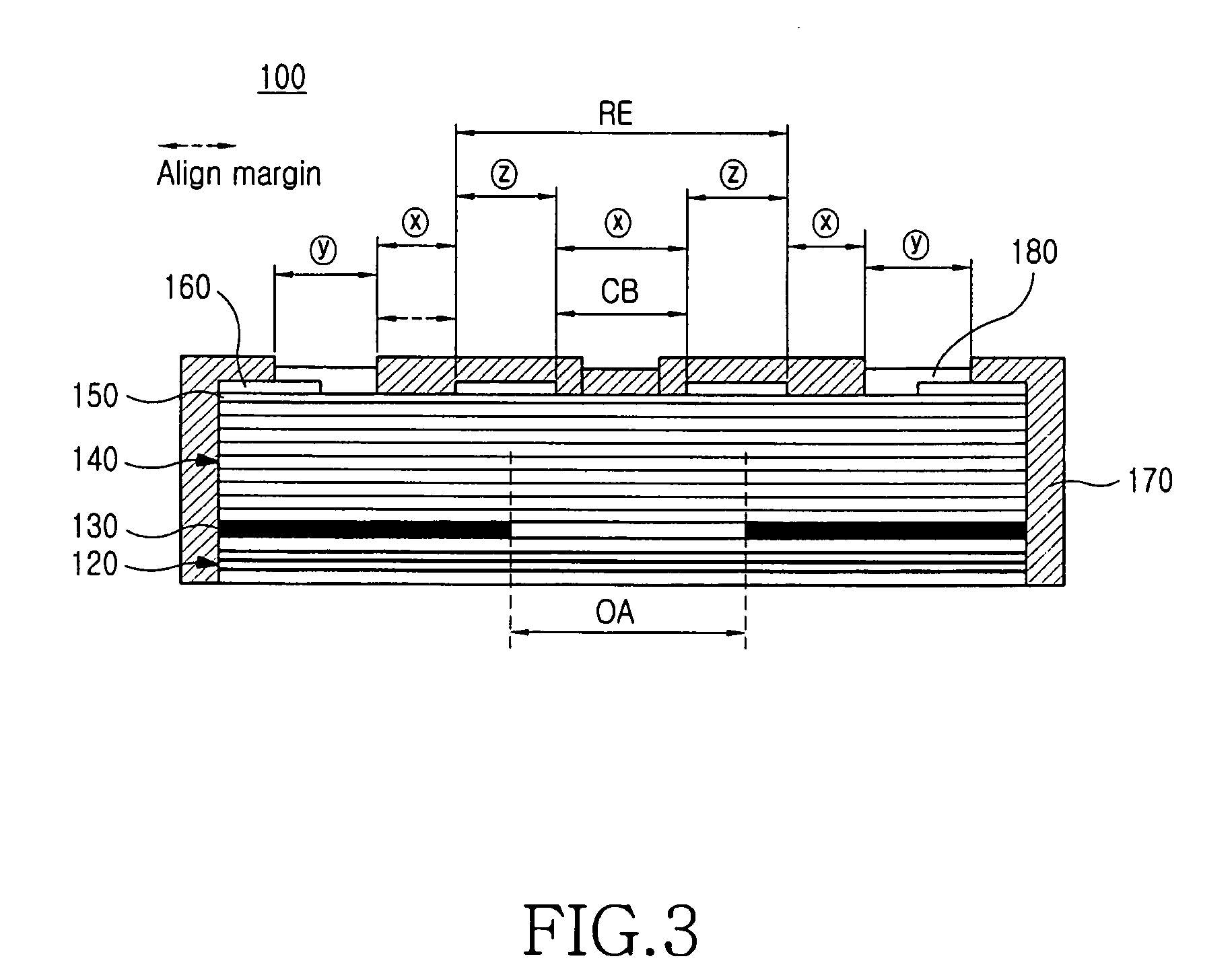
[0014]Therefore, an exemplary aspect of the present invention is to provide a dielectric coating structure, the transmittance of which is not varied on an area where a ¼ wavelength layer area exists and on an area formed by etching the ¼ wavelength layer before and after an index-matching gel is coated. In addition, by forming a ring-shaped aperture structure through the steps of aligning a photoresist and etching the ¼ wavelength layer at an initial stage of a VCSEL fabricating process, an oxide aperture formed due to the formation of a current blocking layer, and a ring-shaped aperture, can be accurately aligned.

Problems solved by technology

As a result, the VCSEL cannot exhibit a stable optical coupling characteristic.
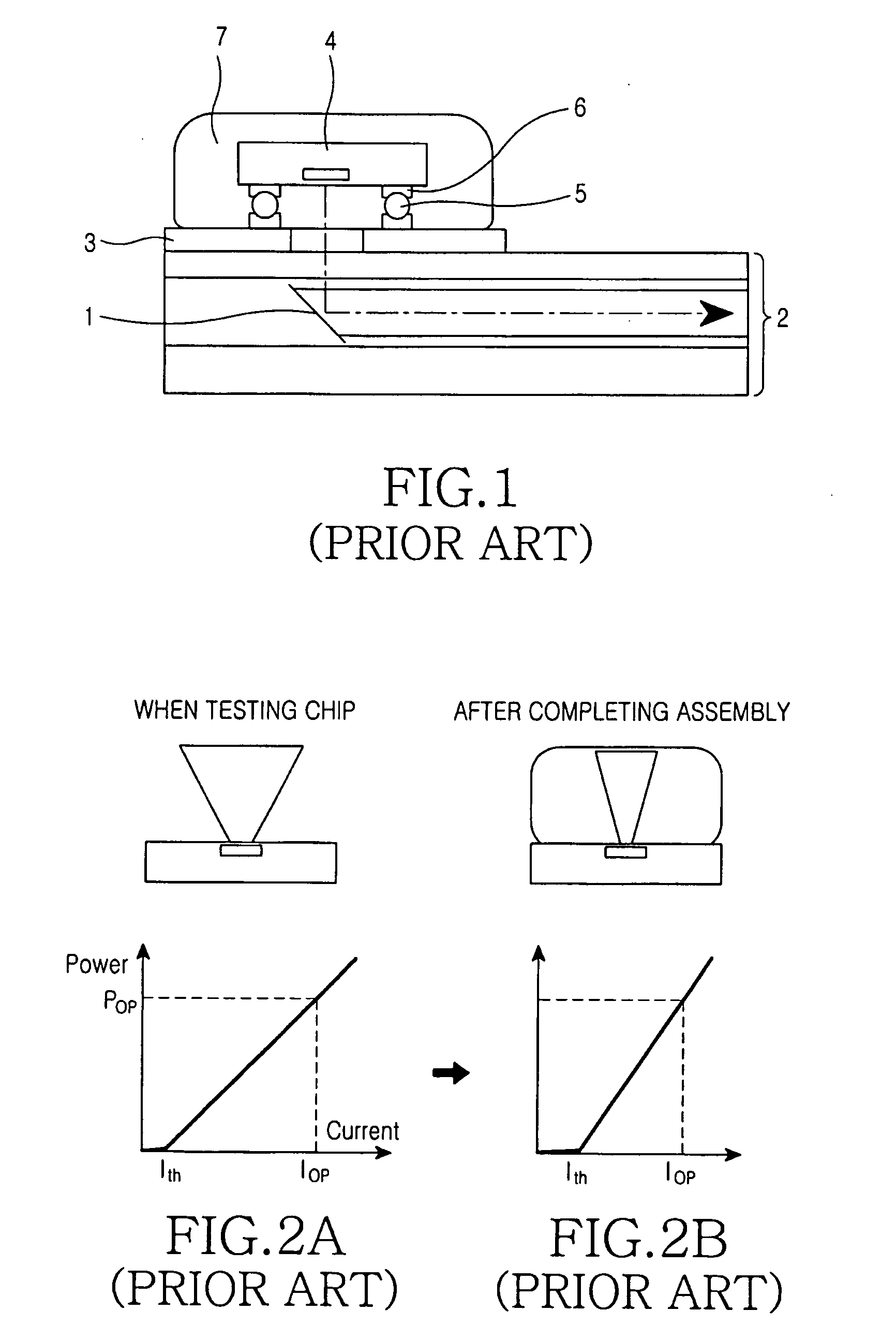
In particular, if the index of the surface of the VCSEL is partially tuned so as to improve the radiation characteristic of the VCSEL, it is difficult to implement a low radiation angle characteristic because the radiation characteristic is greatly varied when the index-matching gel is coated on said surface.

Method used


Image

  • Vertical cavity surface-emitting laser and method of fabricating the same
  • Vertical cavity surface-emitting laser and method of fabricating the same
  • Vertical cavity surface-emitting laser and method of fabricating the same

Examples


Embodiment Construction

[0027]Hereinafter, exemplary embodiments of the present invention will be described with reference to the accompanying drawings. For the purposes of clarity and simplicity, a detailed description of known functions and configurations incorporated herein will be omitted as it may make the subject matter of the present invention rather unclear.

[0028]FIG. 3 shows a structure of a VCSEL according to an exemplary embodiment of the present invention, in which the VCSEL includes a ring-shaped aperture. With regard to FIG. 3, this drawing only shows an area related to an oxide aperture (OA) and an uppermost DBR. In practice, known structures, such as p, n electrodes, a polyimide layer, etc., may be applied when fabricating a VCSEL chip. The description of known structures and functions will be omitted so as not to obscure the invention with description of such known functions and structures. In addition, although description of the present embodiment relates to a VCSEL having an oscillating...


PUM


Abstract

A vertical cavity surface-emitting laser (VCSEL) and a method of fabricating the same with easier alignment of a light output side aperture and an oxide aperture, The VCSEL includes: lower and upper reflection layers laminated with each other and forming a longitudinal resonance section there between; an active layer for producing a laser beam, an electrode formed in a ring shape on the upper reflection layer so the electrode has an aperture through which the laser beam is projected; a contact layer formed on the upper reflection layer; a ¼ wavelength layer formed on the contact layer such that a high transmittance area with the highest transmittance for the laser beam is formed within the aperture of the electrode; and a dielectric layer covering the contact layer and the ¼ wavelength layer, except for the electrode formed part.

Description

CLAIM OF PRIORITY[0001]This application claims the benefit under 35 U.S.C. §119(a) from an application entitled “Vertical Cavity Surface-Emitting Laser and Method of Fabricating the Same,” filed in the Korean Intellectual Property Office on Dec. 20, 2006 and assigned Serial No. 2006-130902, the contents of which are hereby incorporated by reference in its entirety.BACKGROUND OF THE INVENTION[0002]1. Field of the Invention[0003]The present invention relates to a vertical cavity surface-emitting laser (VCSEL) and a method of fabricating the same.[0004]2. Description of the Related Art[0005]A VCSEL is a laser having a resonance cavity mainly including a multi-quantum well sandwiched between two distributed Bragg reflectors (DBRs), wherein the laser obtains a gain in output through current injection. Such a VCSEL is useful in fabricating low-priced optical modules because it exhibits circular radiation of a small angle in general. In particular, VCSELs with an 850 nm oscillating wavelen...

Claims


Application Information

Patent Timeline
IPC IPC(8): H01S3/083
CPCH01S5/0287H01S5/0421H01S5/0425H01S5/18311H01S2301/163H01S5/18369H01S5/18377H01S5/18391H01S5/18327H01S2301/176
Inventor KIM, INLEE, EUN-HWAKIM, SUNG-WON
Owner SAMSUNG ELECTRONICS CO LTD
Learn More