Contact planarization apparatus

a technology of contact and apparatus, which is applied in the direction of photomechanical equipment, grinding drives, instruments, etc., can solve the problems of reducing the final yield and performance of ic devices, non-planar surfaces becoming unsuitable for constructing the next structural layer, and reducing the efficiency of ic devices, so as to achieve precise control of the planarization process, reduce the effect of thermal mass, and effectively sweep out and eliminate entrapped air bubbles

Inactive Publication Date: 2008-06-26
BREWER SCI
View PDF32 Cites 10 Cited by
  • Summary
  • Abstract
  • Description
  • Claims
  • Application Information

AI Technical Summary

Benefits of technology

[0012]One embodiment of the present invention is a planarization apparatus broadly including a lower membrane assembly, an upper membrane assembly, a differential pressure assembly, and a curing or reflowing assembly. The apparatus is designed to efficiently contact planarize coatings applied to individual substrates, such as microelectronic, optoelectronics, photonic, optical, flat panel display, microelectromechanical systems (MEMS), biochips and sensor devices.
[0020]The upper sheet is then deflected downward toward the substrate by reducing the vacuum level in the top pressure chamber. Because the ends of the flexible sheet are held between the curing or reflowing assembly and the lower membrane assembly, the greater vacuum forces in the bottom and central pressure chambers draw the central region of the upper sheet downward toward the center of the substrate.
[0024]By constructing a contact planarization apparatus as described herein, numerous advantages are realized. For example, by using an upper membrane assembly with an upper flexible sheet, a lower membrane assembly with a lower flexible sheet, and a differential pressure assembly for effecting relative movement of the upper and lower sheets, more precise control of the planarization process can be achieved. The differential pressure assembly also provides more complete evacuation of air from inside the apparatus while simultaneously applying the optimal pressure to the substrate and its coating to more effectively sweep out and eliminate entrapped air bubbles between the substrate and the upper sheet. Additionally, by effecting full planarization of the substrate with two flexible sheets rather than a rigid optical flat and a rigid substrate support assembly, less thermal mass is interposed between the curing or reflowing assembly and the substrate, dramatically reducing the overall curing or reflowing time and increasing the throughput of the apparatus.

Problems solved by technology

However, if the surface is not planar, materials may not coat with a uniform thickness.
Unfortunately, non-planar surfaces reduce the final yield and performance of IC devices.
Moreover, at some point of applying successive layers of structure to a non-uniform surface of an IC, the non-planar surface becomes unsuitable for constructing the next structural layer.
Prior art devices suffer from several limitations.
This substantially increases the cure time of the coating applied to the substrate, and thus reduces the throughput of the apparatus.
Another disadvantage of prior art contact planarization devices is that much of the planarization is achieved by sandwiching the substrate and its planarizable coating between a rigid substrate support assembly and a rigid optical flat assembly or other backing.
Sandwiching the substrate between rigid structures to effect much of the planarization makes it difficult to precisely control the pressure applied to the substrate and its coating and the targeting of the pressure.
Many prior art contact planarization devices also do not sufficiently evacuate air from the area around the substrate during planarization, causing unwanted air bubbles to be entrapped in the coating.

Method used


Image

  • Contact planarization apparatus
  • Contact planarization apparatus
  • Contact planarization apparatus

Examples


Embodiment Construction

[0036]The following detailed description of the invention references the accompanying drawings that illustrate specific embodiments in which the invention can be practiced. The embodiments are intended to describe aspects of the invention in sufficient detail to enable those skilled in the art to practice the invention. Other embodiments can be utilized and changes can be made without departing from the scope of the present invention. The following detailed description is, therefore, not to be taken in a limiting sense. The scope of the present invention is defined only by the appended claims, along with the full scope of equivalents to which such claims are entitled.

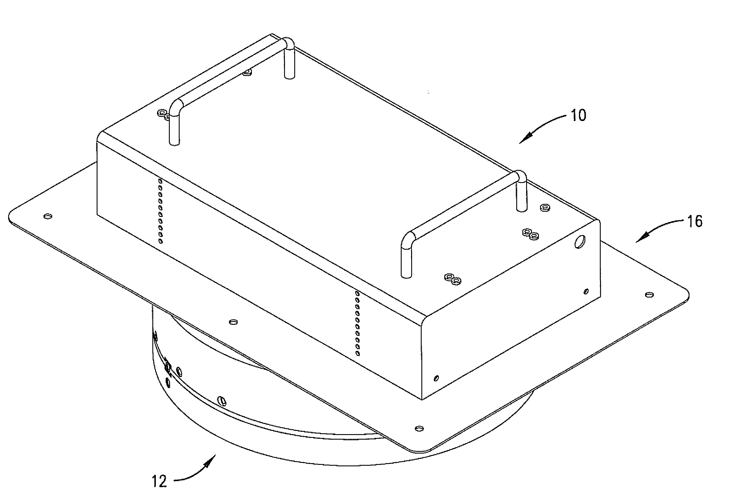
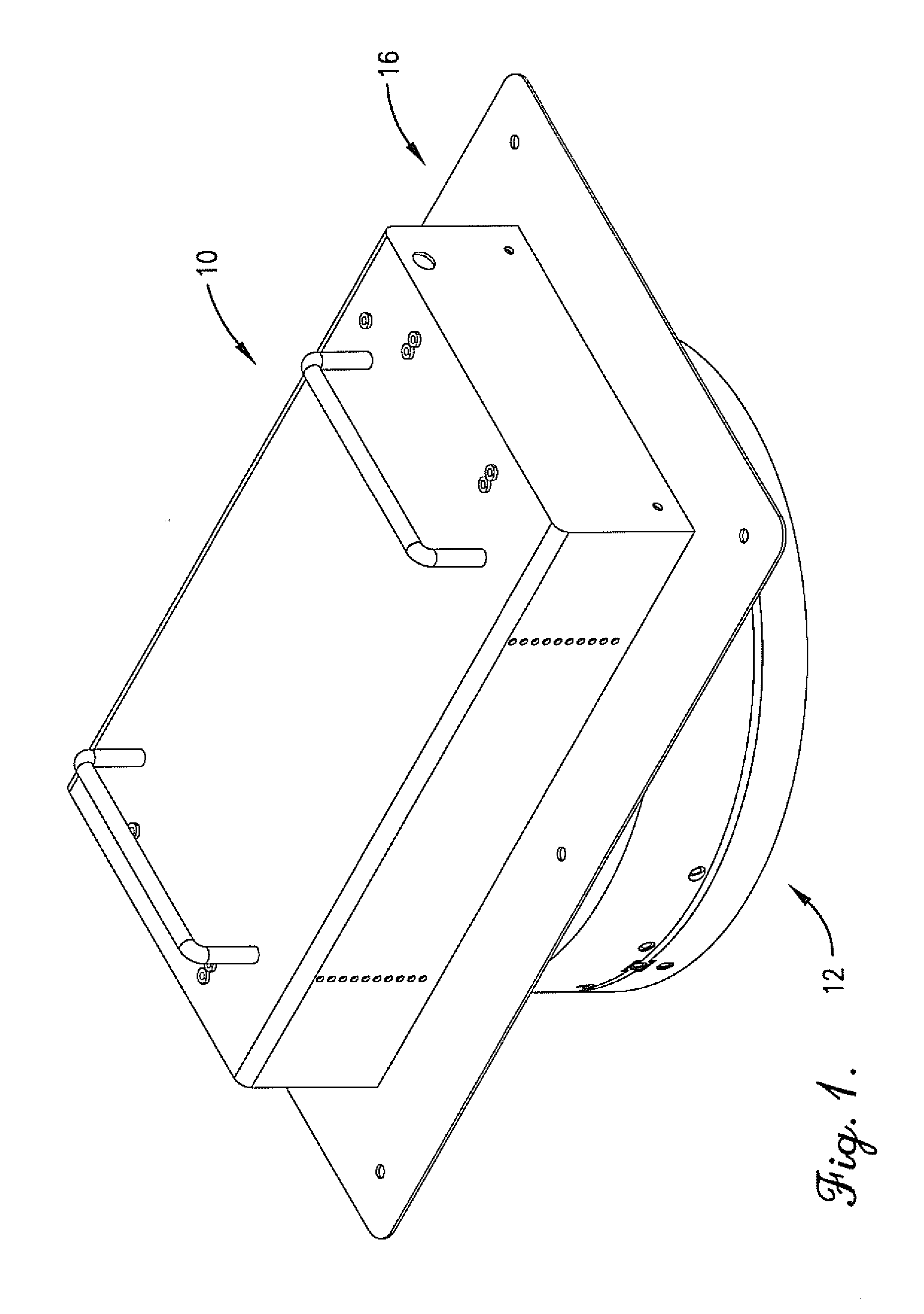
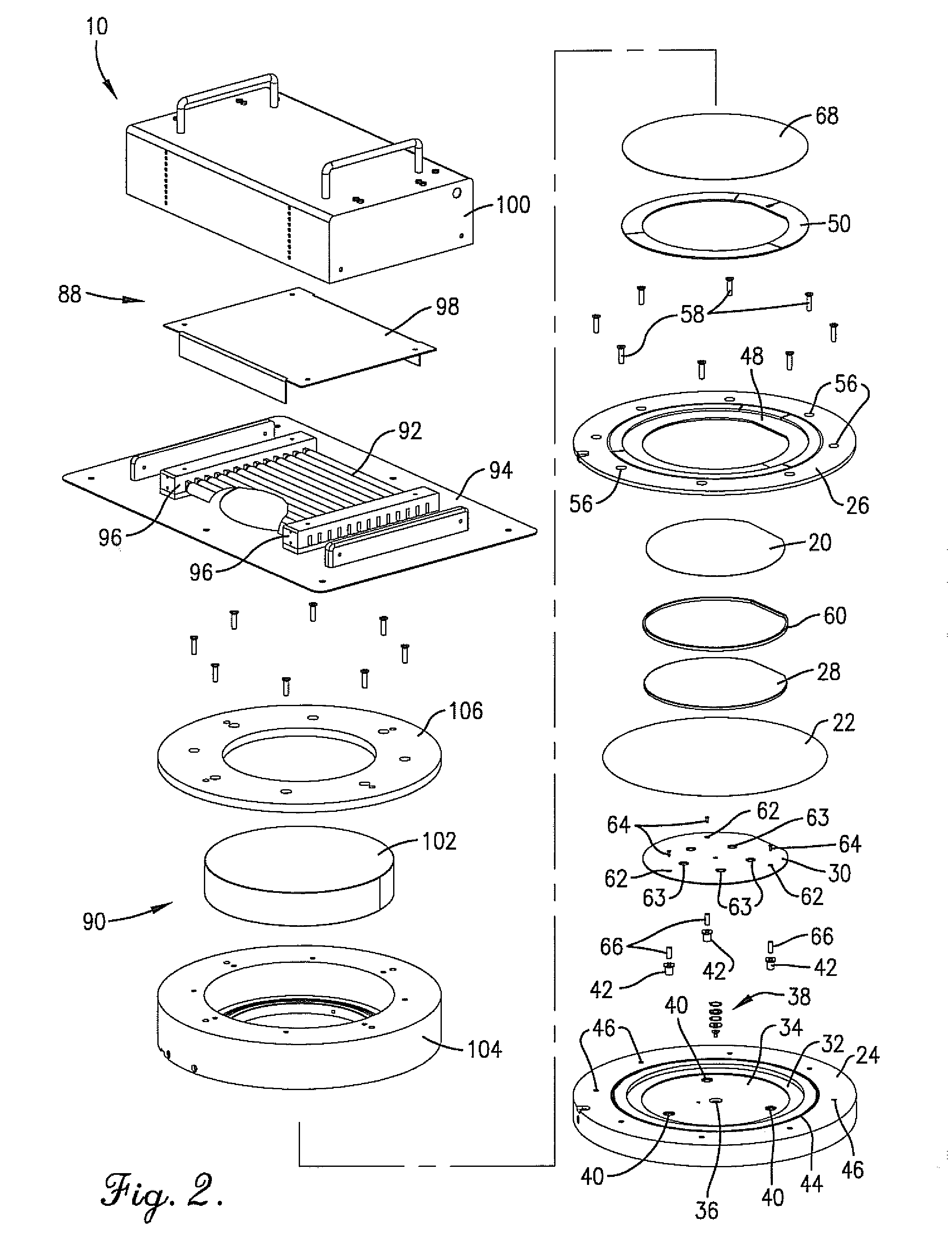
[0037]Turning now to the drawing figures, a planarization apparatus 10 constructed in accordance with a preferred embodiment of the invention is illustrated. The apparatus 10 is designed to efficiently contact planarize coatings applied to individual substrates, such as microelectronic, optoelectronics, photonic, optica...


PUM

PropertyMeasurementUnit
pressureaaaaaaaaaa
pressureaaaaaaaaaa
pressureaaaaaaaaaa

Abstract

A contact planarization apparatus includes a lower membrane assembly, an upper membrane assembly, a differential pressure assembly, and a curing or reflowing assembly. The lower membrane assembly supports a substrate to be planarized and biases it toward the upper membrane assembly under the influence of the pressure differential assembly. The upper membrane assembly planarizes the coating on the substrate under the influence of the differential pressure assembly and includes a flexible sheet which is supported above the substrate stage and below the curing or reflowing assembly via a vacuum force applied by the differential pressure assembly. The differential pressure assembly moves the lower and upper membrane assemblies relative to one another to planarize the coating on the substrate entirely through the application of vacuum and pressure forces. The differential pressure assembly includes atop pressure chamber positioned above the upper face of the upper sheet, a bottom pressure chamber positioned below the lower face of the lower sheet, and a central pressure chamber positioned generally between the lower face of the upper sheet and the upper face of the lower sheet.

Description

BACKGROUND OF THE INVENTION[0001]1. Field of the Invention[0002]The present invention relates to improved methods and apparatus for the contact planarization of surfaces such as those developed during the manufacture of advanced integrated circuits and other devices.[0003]2. Description of the Prior Art[0004]Advanced integrated circuit (IC) designs are highly dependent on complex device-layering techniques to produce semiconductor devices that are more powerful, have lower profiles, and require less energy to operate. To make these qualities possible, more circuits with much finer structures must be integrated into a microchip by constructing multiple layers of interconnects and dielectrics on a semiconductor substrate in an appropriate sequence. Currently, photolithography is the predominant technique used to pattern these ultra-fine structures. This technique requires materials to be deposited and removed from the surface to construct such ultra-fine structures.[0005]Photolithogra...

Claims


Application Information

Patent Timeline
Patent Type & Authority Applications(United States)
IPC IPC(8): B24B41/06
CPCG03F7/168H01L21/67115H01L21/67092H01L21/304
Inventor MCCUTCHEON, JEREMY W.BROWN, ROBERT D.
Owner BREWER SCI
Why Eureka
Try Eureka