Antenna and semiconductor device having the same

Inactive Publication Date: 2008-07-03
SEMICON ENERGY LAB CO LTD
View PDF6 Cites 35 Cited by
  • Summary
  • Abstract
  • Description
  • Claims
  • Application Information

AI Technical Summary

Benefits of technology

[0020]An antenna of the present invention is a conductive structure which has a loop-like shape and has a cut portion in addition to a power feeding portion. In the cut portion, cross-sectional surfaces of the conductive structure face each other. Since electric charge can be accumulated in the cut portion, current flowing into the vicinity of the cut portion becomes large. Therefore, unevenness in current distribution in the conductive structure serving as the antenna is reduced, so that a magnetic field with reduced distortion can be generated in electromagnetic wave transmission and reception to and from the antenna. Accordingly, variation in communication distance and response frequency depending on positions of a semiconductor device having the antenna which is held over a reader/writer can be reduced.
[0021]Further, the antenna provided according to the present invention does not use a circuit element and is formed only by a conductive material; therefore, the antenna can be formed in one plane. Accordingly, the semiconductor device can be easily thinned and can be mounted over various products.
[002

Problems solved by technology

An antenna for an electromagnetic induction method using a high-frequency wave, as described above, has a quite short wavelength which is approximately equal to the length of the antenna; therefore, there arises a problem such that current density distribution in the antenna becomes uneven.
In a loop antenna, this un

Method used


Image

  • Antenna and semiconductor device having the same
  • Antenna and semiconductor device having the same
  • Antenna and semiconductor device having the same

Examples


embodiment mode 1

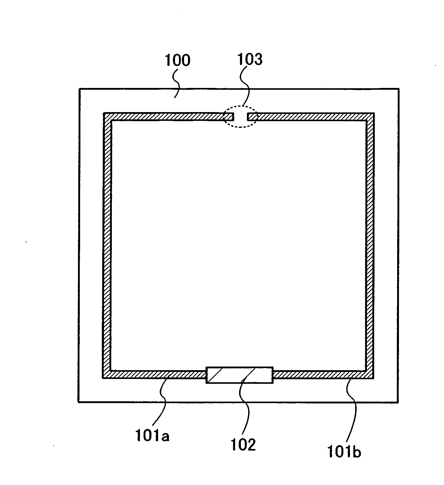
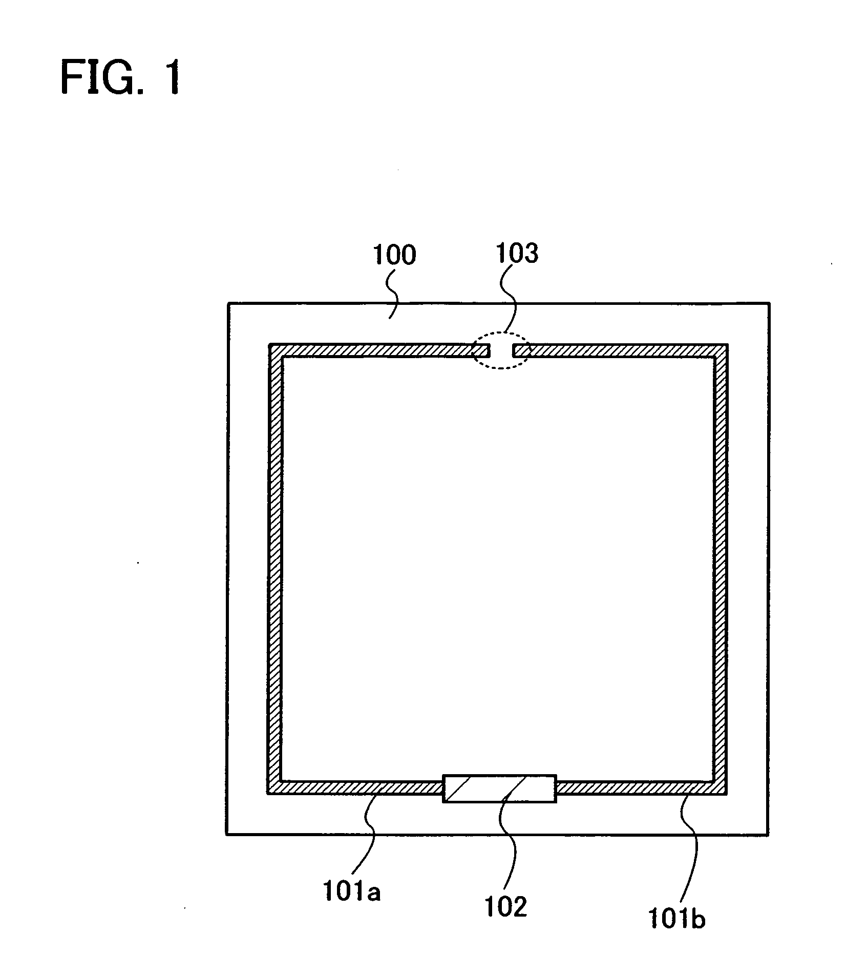
[0047]In this embodiment mode, a mode of an antenna of the present invention is described with reference to the drawings.

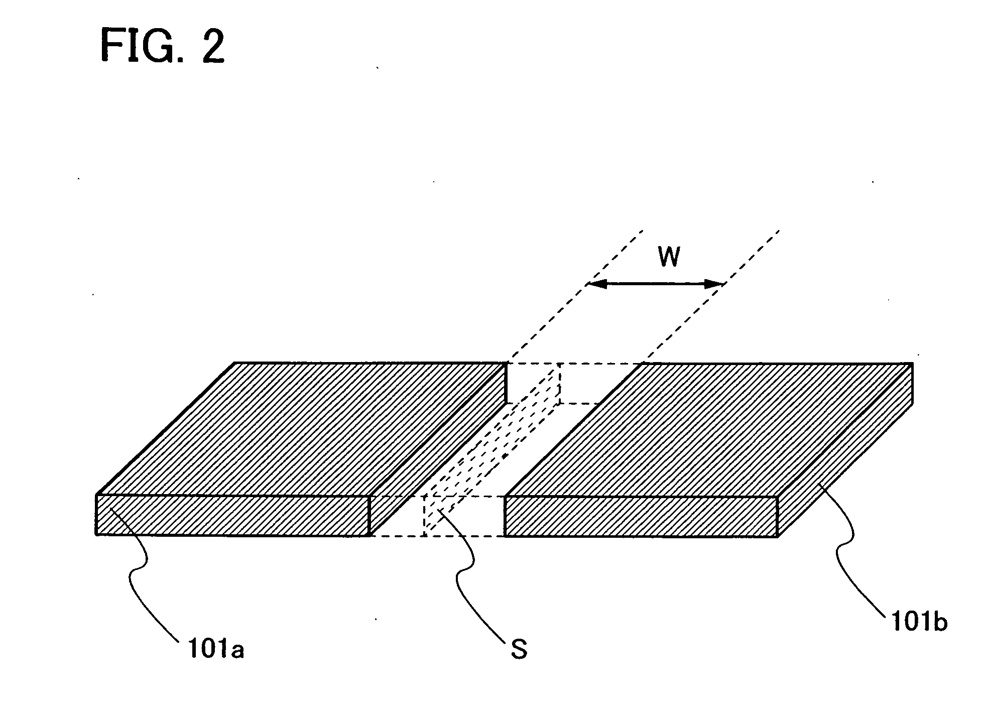
[0048]An antenna described in this embodiment mode includes a substrate 100, a conductive structure 101a and a conductive structure 101b, a power feeding portion 102, and a cut portion 103, as shown in FIG. 1. The antenna has a region in which an end portion of the conductive structure 101a and an end portion of the conductive structure 101b face each other. Note that the substrate 100 is not necessary in some cases. The antenna may only include, for example, the conductive structure 101a, the conductive structure 101b, the power feeding portion 102, and the cut portion 103.

[0049]The antenna in this embodiment mode is used for an electromagnetic induction method. In the electromagnetic induction method, change in a magnetic field generated by an antenna is converted into current. Therefore, when the antenna has a loop-like shape, the number of magnetic fluxes can ...

embodiment mode 2

[0089]This embodiment mode describes a semiconductor device having the antenna described in the foregoing embodiment mode with reference to FIGS. 7A to 7C. Specifically, description is made of the case where a semiconductor device is formed by attaching an element layer (also called an IC chip) having elements such as transistors to the antenna described in the foregoing embodiment mode. FIG. 7B is an enlarged view of a region 120 in FIG. 7A, and FIG. 7C is a cross-sectional view along the line a-b in FIG. 7B.

[0090]First, the conductor structures 101a and 101b serving as an antenna and the power feeding portions 102a and 102b are formed over the substrate 100. Meanwhile, an element layer 126 having elements such as transistors is formed separately from the antenna. For the antenna, an antenna having any structure described in the foregoing embodiment mode may be employed. The element layer 126 includes an integrated circuit portion 131 having elements such as transistors and conduct...

embodiment mode 3

[0096]This embodiment mode describes a method of manufacturing the semiconductor device described in Embodiment Mode 2, with reference to drawings. In this embodiment mode, description is made of the case where an element layer is formed by providing elements such as transistors over a flexible substrate.

[0097]First, a release layer 702 is formed over a surface of a substrate 701. Then, an insulating film 703 serving as a base and an amorphous semiconductor film 704 (e.g., a film containing amorphous silicon) are formed thereover (see FIG. 8A). Note that the release layer 702, the base insulating film 703, and the amorphous semiconductor film 704 can be formed consecutively.

[0098]The substrate 701 may be a glass substrate, a quartz substrate, a metal substrate, or a stainless steel substrate that has an insulating film formed over its surface, a thermally stable plastic substrate that can withstand the processing temperature during the manufacturing process, or the like. When such a...


PUM


Abstract

An antenna for an electromagnetic induction method, in which unevenness in current density distribution is suppressed so that a magnetic field with reduced distortion is generated. In addition, a semiconductor device with less variation in response frequency and communication distance is also provided. The antenna has a loop-like shaped conductive structure with a cut portion in a part thereof and cross-sectional surfaces of the conductive structure face each other in the cut portion. In addition, the conductive structure of the antenna is electrically coupled to have capacity in the cut portion. The semiconductor device has the antenna and an integrated circuit which is connected to the antenna in a power feeding portion.

Description

BACKGROUND OF THE INVENTION[0001]1. Field of the Invention[0002]The present invention relates to an antenna which transmits and receives information in an electromagnetic induction method and a semiconductor device having the antenna.[0003]2. Description of the Related Art[0004]In recent years, RFID (radio frequency identification) systems have been researched and put into practical use.[0005]RFID refers to a technique of contactless communication in order to store or to read data, between a reader / writer and a semiconductor device capable of wireless information transmission and reception (such a semiconductor device is also called an RFID tag, an ID tag, an IC tag, an IC chip, a wireless tag, an electronic tag, or a wireless chip).[0006]As a communication method of such RFID, a radio wave method or an electromagnetic induction method is mainly used (e.g., see Non-Patent Document 1: illustrated RFID Textbook All about Wireless IC Tags Directed to Ubiquitous Society—, editorial supe...

Claims


Application Information

Patent Timeline
IPC IPC(8): H01Q7/00
CPCH01Q1/2283H01Q7/00H01Q1/38
Inventor YAKUBO, YUTOKOEN, TAKAAKI
Owner SEMICON ENERGY LAB CO LTD
Why Eureka
Try Eureka