Graphene channel silicon carbide power semiconductor transistor

a silicon carbide and semiconductor technology, applied in the direction of semiconductor devices, basic electric elements, electrical equipment, etc., can solve the problems of large off-state leakage current, low breakdown voltage, low reliability, etc., and achieve the effect of reducing the overall off-state leakage current, enhancing the function of assisting depletion, and improving breakdown voltag

Active Publication Date: 2021-10-26
SOUTHEAST UNIV
View PDF5 Cites 0 Cited by
  • Summary
  • Abstract
  • Description
  • Claims
  • Application Information

AI Technical Summary

Benefits of technology

[0010]According to the present invention, the graphene strip is embedded in the surface of the P-type body region, and the graphene is contacted with the surface of the gate oxide, and is distributed in a cellular manner in the gate width direction; at the moment, a conducting channel of a device is still made of the graphene, and in the case of maintaining basically invariable on-resistance and current transmission capacity, the P-type body regions are separated by the graphene strip, thus enhancing the function of assisting depletion, which further reduces the overall off-state leakage current of the device, and improves the breakdown voltage.
[0011](1) The graphene strip is distributed in a cellular manner, so that the P-type body regions are separated, and are in multi-surface contact with the graphene, and in the case of a zero gate voltage and a high leakage voltage, electrons are present in the graphene and are recombined with majority carrier holes of the P-type body region to form a space charge region, thus enhancing the function of assisting depletion, which further reduces the overall off-state leakage current of the device. Therefore, compared with a semiconductor device with graphene continuously distributed in the gate oxide, the device has a smaller off-state leakage current, a higher breakdown voltage and stronger reliability.
[0012](2) The cellular graphene array is embedded in the P-type body region; when a positive voltage is applied to a drain electrode of the device, majority carrier electrons of the N+-type source region will be directly injected into the N-type drift region and the N-type substrate through the graphene channel and finally reach a drain end to form a current path. Due to different carrier mobilities of the silicon carbide and the graphene, when the graphene is distributed at intervals in the gate oxide, the device has a higher on-resistance and uneven current transmission. Therefore, compared with a device with graphene distributed at intervals in the gate oxide, the device has a lower on-resistance, a better on-state I-V characteristic, and a stronger current transmission capability. Compared with a device with graphene continuously distributed in the gate oxide, the present invention has a basically unchanged on-resistance and a basically unchanged current transmission capability.
[0013](3) A silicon carbide epitaxial growth method is one of the methods for preparing the graphene, and a silicon carbide single crystal is heated at high temperature to cause graphitization, thus obtaining the graphene with excellent performance based on a silicon carbide substrate, which is compatible with the existing device preparation process.
[0014](4) Since a carrier mobility of a graphene material is less affected by temperature, the graphene channel is adopted in the proposed graphene channel silicon carbide power semiconductor transistor, carrier transmission in the channel is less affected by temperature, and on-resistance stability is better at high temperature.

Problems solved by technology

However, the continuous high mobility graphene layer has large current density, and the conducting channel of the device cannot be completely exhausted under the conditions of high leakage voltage and zero gate voltage, resulting in a large off-state leakage current, a low breakdown voltage and low reliability.

Method used


Image

  • Graphene channel silicon carbide power semiconductor transistor
  • Graphene channel silicon carbide power semiconductor transistor
  • Graphene channel silicon carbide power semiconductor transistor

Examples


example 1

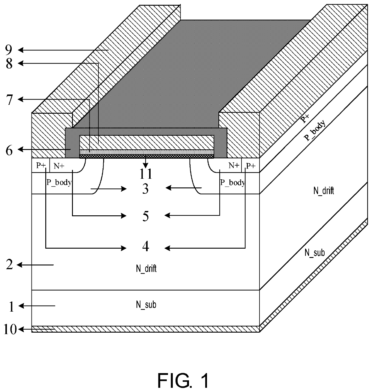
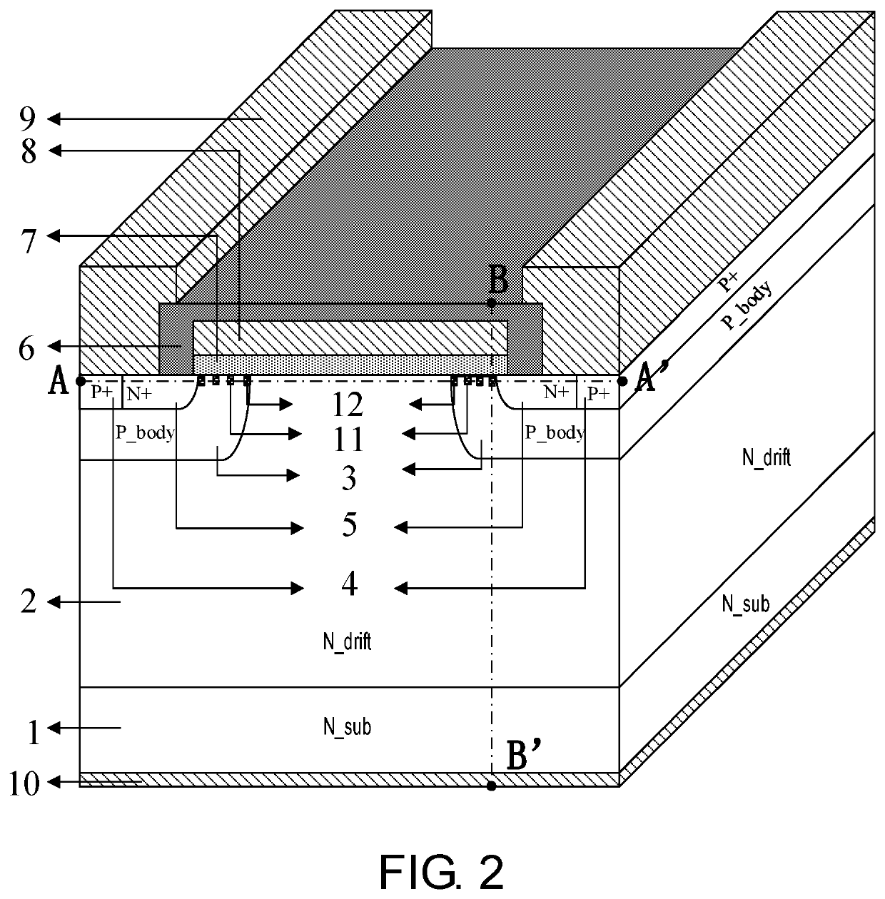
[0035]A graphene channel silicon carbide power semiconductor transistor comprises an N-type substrate 1, wherein one side of the N-type substrate 1 is provided with a drain metal 10, and the other side of the N-type substrate 1 is an N-type drift region 2, a pair of P-type body regions 3 are arranged at two ends of the N-type drift region 2, a P+-type body contact region 4 and an N+-type source region 5 are respectively arranged in each of the P-type body regions 3, a gate oxide layer 7 is arranged on a surface of the N-type drift region 2, and two ends of the gate oxide layer 7 are respectively extended into the P-type body regions 3 at the two sides, a polysilicon gate 8 is arranged on a surface of the gate oxide layer 7, a passivation layer 6 is arranged on the polysilicon gate 8, and the passivation layer 6 wraps two sides of the polysilicon gate 8, and a source metal 9 is arranged on the N+-type source region 5 and the P+-type body contact region 4.

[0036]In the present embodime...

example 2

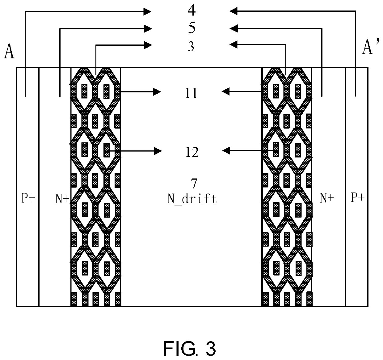
[0037]In the present embodiment, based on a traditional device structure, graphene embedded in the P-body region 3 is extended from an intersection of the N+-type source region 5 and the P-body region 3 to the N-type drift region 5 at intervals in a gate length direction, and a graphene block 12 has a length of 0.1 μm, an interval of 0.1 μm, and a thickness of 1 nm; and a graphene strip 11 is distributed continuously or at intervals in a gate width direction.

[0038]Compared with the device in the Example 2 with graphene distributed continuously or at intervals, the device in the first embodiment in cellular distribution with graphenes interconnected in the gate width direction has a lower on-resistance and a stronger current transmission capability. The cellular graphene makes a gap between the P-type body regions more obvious, an assisting depletion effect stronger, an off-state leakage current smaller, and a breakdown voltage higher. Therefore, the graphene channel silicon carbide ...


PUM

PropertyMeasurementUnit
gate voltageaaaaaaaaaa
thicknessaaaaaaaaaa

Abstract

The invention provides a graphene channel silicon carbide power semiconductor transistor, and its cellular structure thereof. Characterized in that, a graphene strip serving as a channel is embedded in a surface of the P-type body region and two ends of the graphene strip are respectively contacted with a boundary between the N+-type source region and the P-type body region and a boundary between the P-type body region and the N-type drift region, and the graphene strip is distributed in a cellular manner in a gate width direction, a conducting channel of a device is still made of graphene; in the case of maintaining basically invariable on-resistance and current transmission capacity, the P-type body regions are separated by the graphene strip, thus enhancing a function of assisting depletion, which further reduces an overall off-state leakage current of the device, and improves a breakdown voltage.

Description

CROSS-REFERENCE TO RELATED APPLICATION[0001]This application is a 371 of international application of PCT application serial no. PCT / CN2018 / 107329, filed on Sep. 25, 2018, which claims the priority benefit of China application no. 201810682926.1, filed on Jun. 27, 2018. The entirety of each of the above mentioned patent applications is hereby incorporated by reference herein and made a part of this specification.BACKGROUND OF THE INVENTION1. Technical Field[0002]The present invention belongs to the field of high-voltage power semiconductor devices, and more particularly, to a graphene channel silicon carbide power semiconductor device.2. Background Art[0003]Graphene is a single-layer carbon polymer with a conduction band and a valence band met at a Dirac point, and is called a zero-band gap semiconductor. As a new material, the graphene has the features of extremely high carrier mobility, submicron-scale ballistic transmission characteristic at room temperature, quantum Hall effect,...

Claims


Application Information

Patent Timeline
Patent Type & Authority Patents(United States)
IPC IPC(8): H01L29/16H01L29/78H01L29/06
CPCH01L29/1606H01L29/0607H01L29/1608H01L29/7802H01L29/267H01L29/165H01L29/1095H01L29/66068
Inventor SUN, WEIFENGLIU, SIYANGTANG, LIZHILI, SHENGZHANG, CHIWEI, JIAXINGLU, SHENGLISHI, LONGXING
Owner SOUTHEAST UNIV
Why Eureka
Try Eureka