Method for burst mode, bit line charge transfer and memory using the same

a bit line charge transfer and burst mode technology, applied in the field of methods, can solve the problem of one source of power consumption in the memory device during a read operation, and achieve the effect of reducing the amount of power

Active Publication Date: 2008-07-03
MACRONIX INT CO LTD
View PDF6 Cites 12 Cited by
  • Summary
  • Abstract
  • Description
  • Claims
  • Application Information

AI Technical Summary

Benefits of technology

[0008]In large scale integrated circuit memory devices having modes of operation, such as burst read modes, in which a predictable sequence of bit line decoding is executed during a read cycle, charge from a previously sensed bit line is transferred to a bit line to be sensed next, and re-used. The amount of charge on a previously sensed bit line which can be transferred to a next bit line directly reduces the amount of power needed for pre-charging the next bit line. Thus, the present invention provides for reusing charge during read sequences, and particularly in such sequences that have predictable bit line decoding patterns.

Problems solved by technology

One source of power consumption in memory devices during a read operation arises from bit line pre-charge operations, used to set up a bit line for a read.
Since the bit lines have relatively large capacitance, the pre-charging and discharging operations can require significant current, and substantial power to produce the current.

Method used


Image

  • Method for burst mode, bit line charge transfer and memory using the same
  • Method for burst mode, bit line charge transfer and memory using the same
  • Method for burst mode, bit line charge transfer and memory using the same

Examples


Embodiment Construction

[0021]The following detailed description is made with reference to the figures. Preferred embodiments are described to illustrate the present invention, not to limit its scope, which is defined solely by the claims. Those of ordinary skill in the art will recognize a variety of equivalent variations on the description that follows.

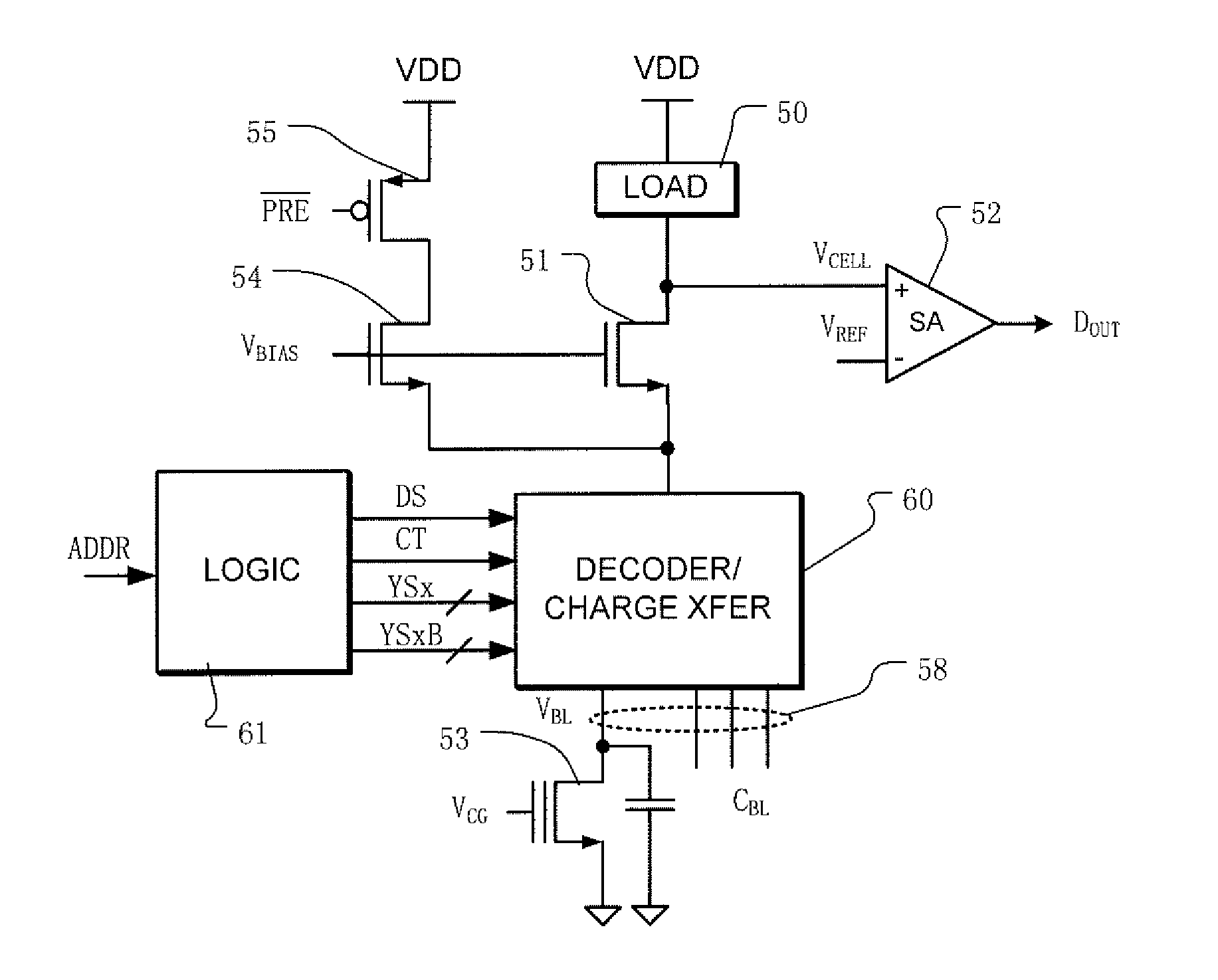
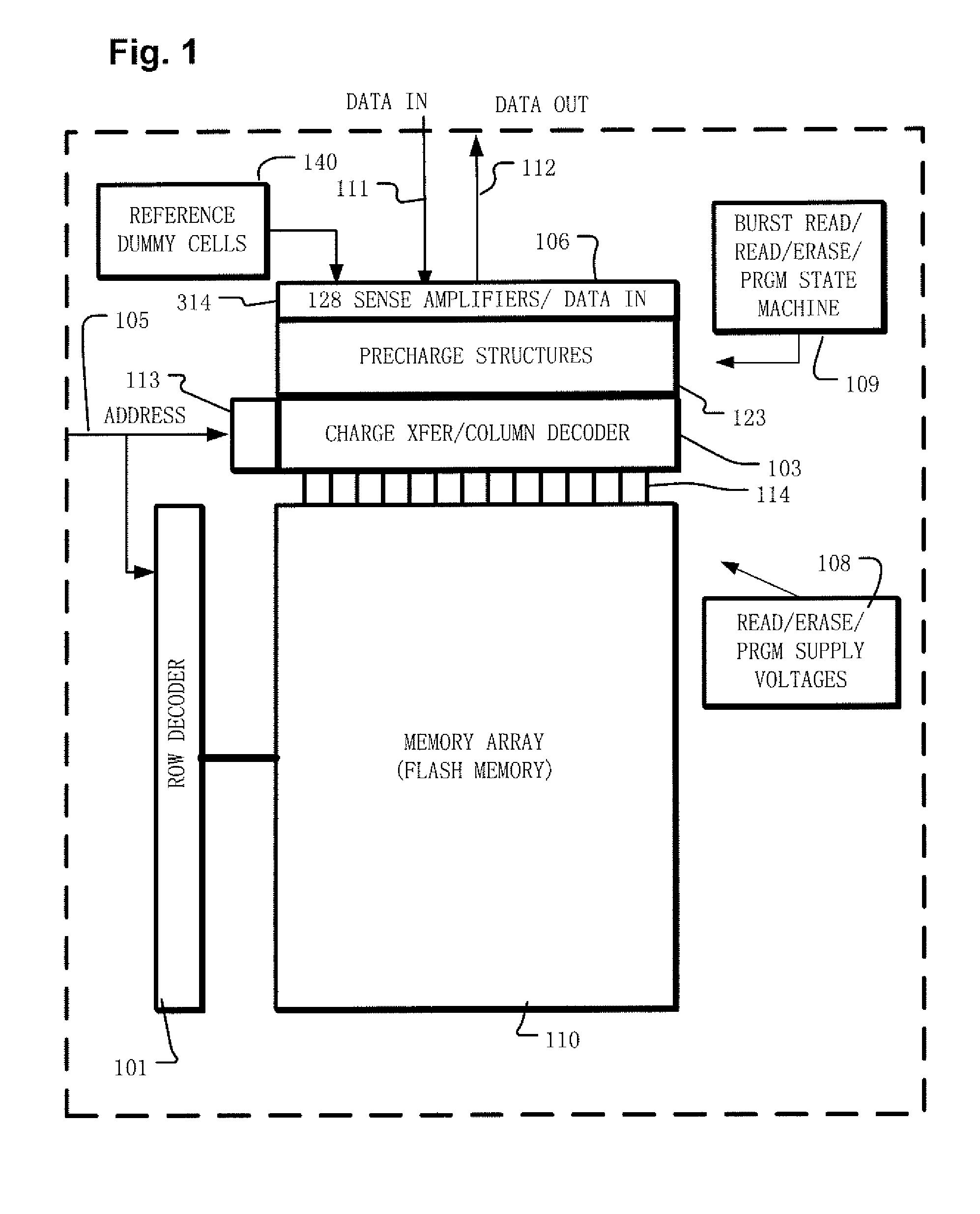
[0022]FIG. 1 is a simplified block diagram of an integrated circuit memory with a burst read mode, and including pre-charge and charge transferring circuitry to support reuse of charge used for sensing as described herein. The integrated circuit includes a memory array 110 implemented using memory cells, such as floating gate or charge trapping non-volatile memory cells flash memory. Read only memory cells or other types of memory cells can also be used in embodiments of the technology. A page / row decoder 101 is coupled to a plurality of word lines arranged along rows in the memory array 110. A column decoder 103, with charge transfer circuitry, is coupled...


PUM


Abstract

A memory device operates according to a method for reading includes pre-charging a first set of selected bit lines to a pre-charge voltage and sensing data from the cells coupled to the first set of selected bit lines. Then, residual charge is transferred from the first set of selected bit lines to corresponding members of a second set of selected bit lines. The second set of selected bit lines, having an initial charge transferred from the first set, is then pre-charged to the pre-charge voltage. The data from the cells coupled to the second set of selected bit lines it is then sensed. In embodiments described herein, the read operation occurs in a burst read mode, where a volume of data having consecutive addresses is read.

Description

BACKGROUND OF THE INVENTION[0001]1. Field of the Invention[0002]The present invention relates generally to integrated circuit memory devices, and more specifically to efficient read methods in such devices with reduced power consumption.[0003]2. Description of Related Art[0004]Power consumption in integrated circuit memory devices is a design concern in many applications, including memory for small portable devices that rely on battery power or other sources of limited power, and memory for systems that otherwise require power efficient operation.[0005]One source of power consumption in memory devices during a read operation arises from bit line pre-charge operations, used to set up a bit line for a read. Typical structures used for these purposes are illustrated in U.S. Pat. No. 6,219.290, entitled MEMORY CELL SENSE AMPLIFIER, invented by Chang et al.; U.S. Pat. No. 6,498,751, entitled FAST SENSE AMPLIFIER FOR NONVOLATILE MEMORIES, invented by Ordonez, et al.; U.S. Pat. No. 6,392,4...

Claims


Application Information

Patent Timeline
Patent Type & Authority Applications(United States)
IPC IPC(8): G11C7/12
CPCG11C7/1018G11C7/1048G11C11/4096G11C11/4094G11C7/12
Inventor LIN, YUNG FENG
Owner MACRONIX INT CO LTD
Why Eureka
Try Eureka