

Method of making a vertical electronic device
a vertical electronic device and processing method technology, applied in the direction of semiconductor/solid-state device manufacturing, electric apparatus, basic electric elements, etc., can solve the problems of increasing the thickness of the bulk wafer, increasing the power consumption, increasing the effort to remove heat, and destroying the device, so as to reduce the amount of power used by the apparatus and reduce the processing time. , the effect of low melting poin
- Summary
- Abstract
- Description
- Claims
- Application Information
AI Technical Summary
Benefits of technology
Problems solved by technology
Method used
Image

Examples
Embodiment Construction
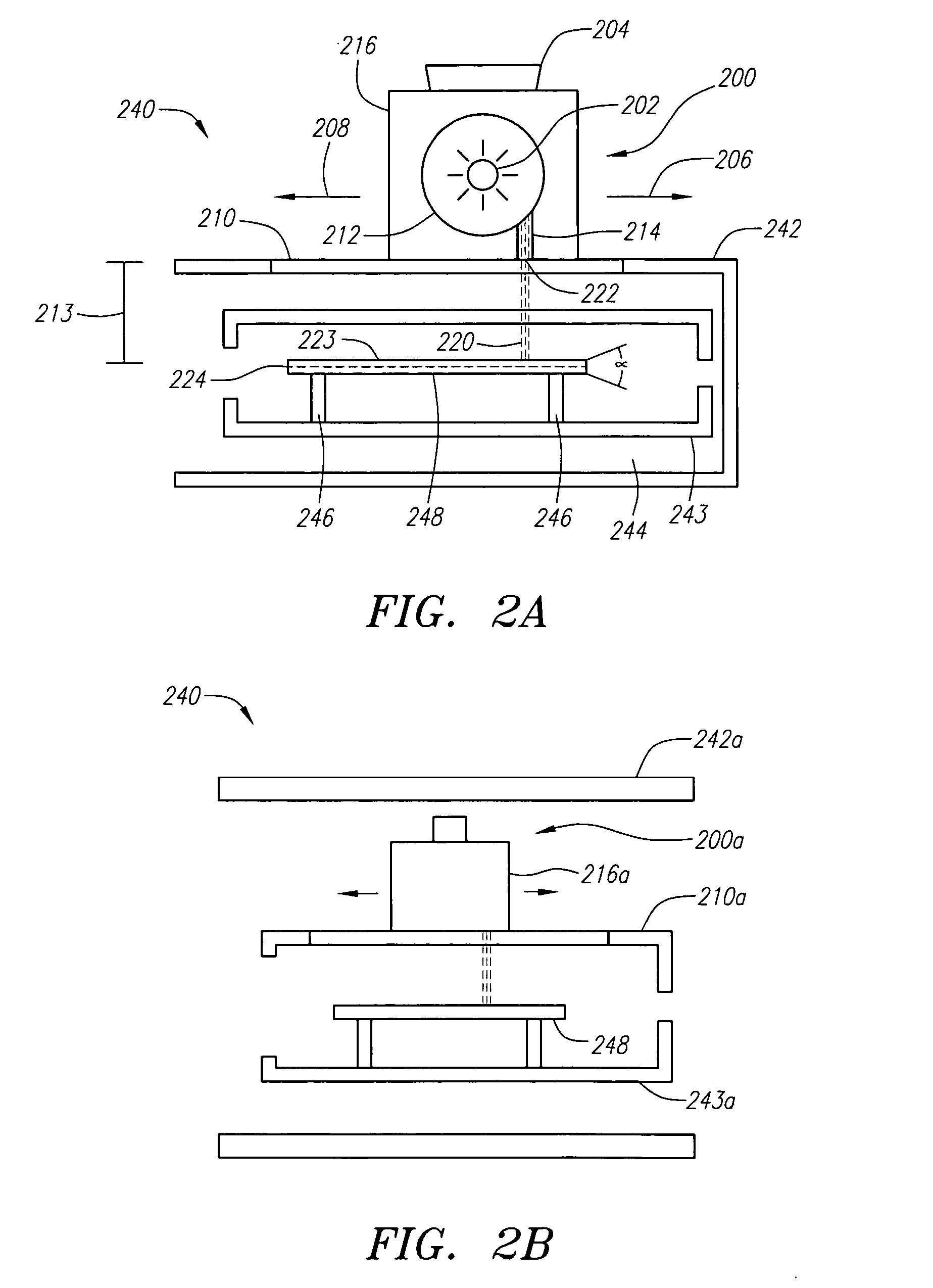
[0034] As used herein, the word “flash” includes it ordinary meaning as generally understood by those of ordinary skill in the art. This definition of flash also includes to give off light suddenly or substantially instantaneous (or in transient bursts) for a duration of time between about 1 nanosecond and about 10 seconds.
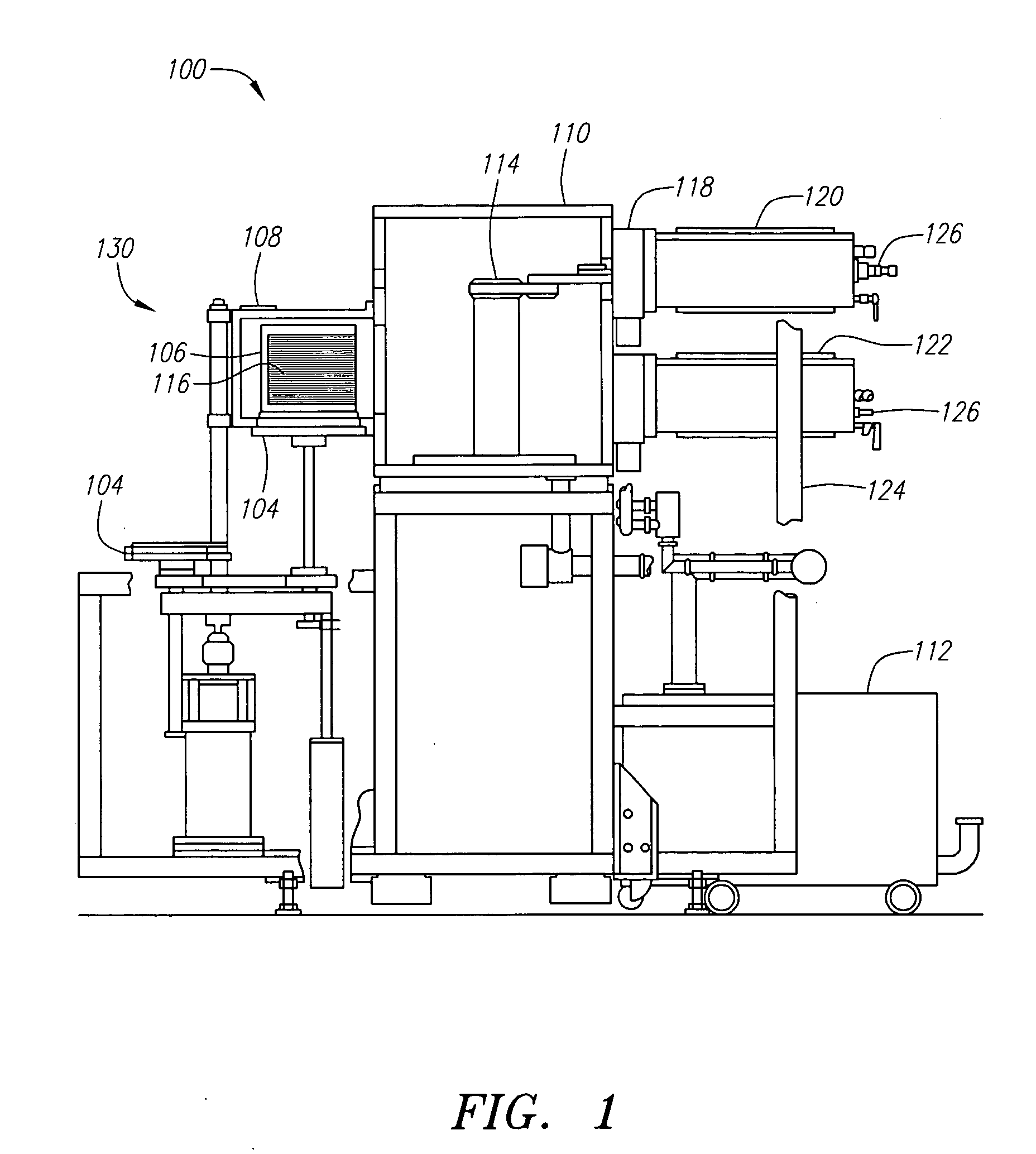
[0035]FIG. 1 is a schematic illustration of a side view of one embodiment of a semiconductor wafer processing system 100 that establishes a representative environment of the present invention. Processing system 100 includes a loading station 130 which has multiple platforms 104 for supporting and moving a wafer cassette 106 up and into a loadlock 108. Wafer cassette 106 may be a removable cassette which is loaded into a platform 104, either manually or with automated guided vehicles (AGV). Wafer cassette 106 may also be a fixed cassette, in which case wafers are loaded onto cassette 106 using conventional atmospheric robots or loaders (not shown). Once wafer cass...
PUM
 Abstract
Description
Claims
Application Information