Semiconductor device

a technology of semiconductor devices and semiconductors, applied in the direction of instruments, digital data processing details, sustainable buildings, etc., can solve the problems of increasing power consumption, inability to perform normal modulation, and unstable electric power, so as to reduce the power consumption of transmitting the signal to the outside, reduce manufacturing cost and manufacturing time, and achieve reliable operation at the time of transmission

Inactive Publication Date: 2007-12-27
SEMICON ENERGY LAB CO LTD
View PDF19 Cites 9 Cited by
  • Summary
  • Abstract
  • Description
  • Claims
  • Application Information

AI Technical Summary

Benefits of technology

[0024]According to the invention, in a semiconductor device having an anti-collision function which repeatedly performs a transmit operation a plurality of times, by using the controller to stop the central processing unit when a signal is transmitted to the outside, the amount of power consumed when transmitting the signal to the outside is reduced. Therefore, when the arithmetic circuit operates simultaneously with the storage device and the modulation circuit, that is, when a communication signal is transmitted from the antenna by the modulation circuit modulating a carrier, electric power can be stabilized and operation at the time of transmission can be performed reliably. Further, in a semiconductor device having a function of repeatedly performing a transmit operation a plurality of times, it is not necessary to remake the semiconductor device from the stage of mask design due to a change in specifications accompanying a change in a method of operation. Therefore, reduction in manufacturing cost and manufacturing time can be achieved. Further, there are no concerns such as whether a semiconductor device remade due to a change in mask design will be defective.

Problems solved by technology

However, there is a problem with the conventional IC chip which includes an arithmetic circuit and a storage device in that due to the size of circuits included in the arithmetic circuit and the storage device, power consumption increases.
Further, there is a problem in that when the arithmetic circuit, the storage device, and the modulation circuit operate simultaneously, that is, when a communication signal is transmitted from the antenna by the modulation circuit modulating a carrier, electric power is not stable and a normal modulation cannot be performed.

Method used


Image

  • Semiconductor device
  • Semiconductor device
  • Semiconductor device

Examples


embodiment 1

[0102]Next, an example of a structure of the above-described semiconductor device will be described, with reference to the drawings. FIG. 9A shows a top view of a semiconductor device of this embodiment, and FIG. 9B shows a cross section taken along the line A-B in FIG. 9A.

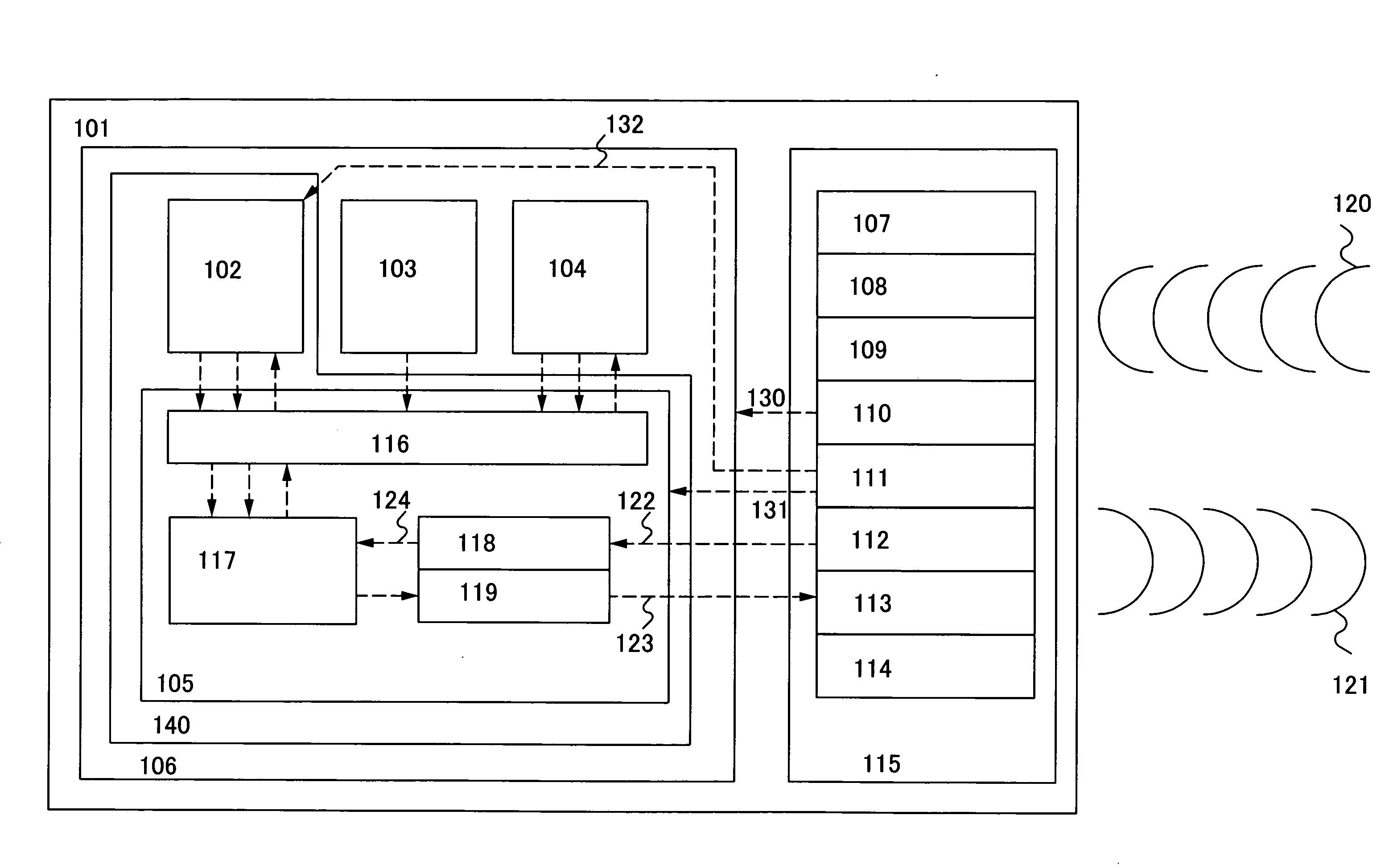
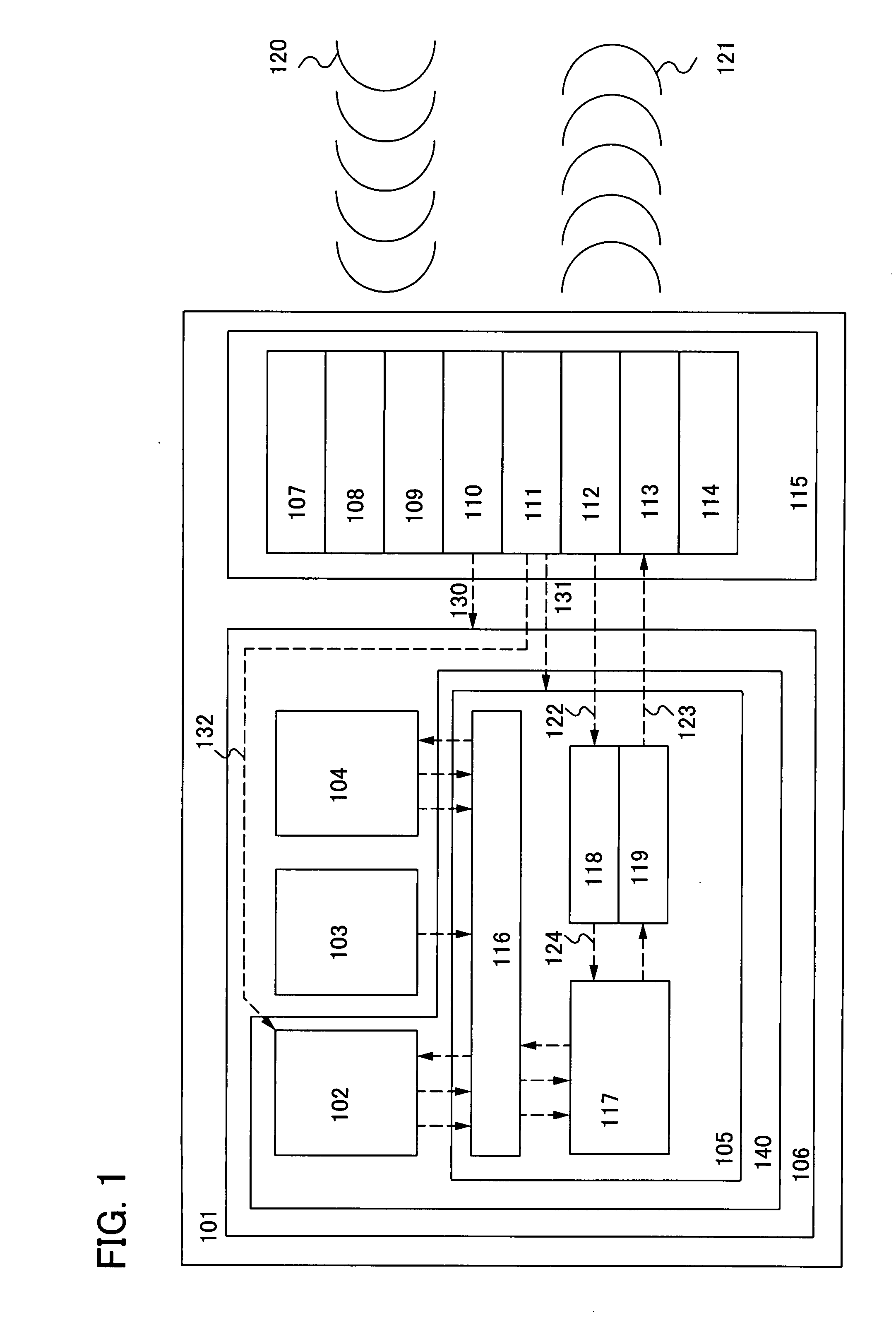
[0103]As shown in FIG. 9A, in the semiconductor device of this embodiment, an integrated circuit 1302 and an antenna 107 are sandwiched between substrates 440 and 441. The integrated circuit 1302 includes the analog portion 115, excluding the antenna 107, and the digital portion 106 which are included in FIG. 1.

[0104]As shown in FIG. 9B, in the semiconductor device 101, the antenna 107 provided over the substrate 441 and an element formation layer 430 provided over the substrate 440 are firmly attached to each other by an anisotropic conductive adhesive 442. Further, the anisotropic conductive adhesive 442 includes an organic resin 443 and conductive particles 444. A connecting terminal 445 of the element formatio...

embodiment 2

[0114]In this embodiment mode, a structure including a booster antenna circuit (hereinafter referred to as a booster antenna) for a semiconductor device described in the embodiment mode and embodiment above will be described with reference to the drawings.

[0115]Note that the booster antenna described in this embodiment refers to an antenna (which is hereinafter referred to as a booster antenna) having a size larger than that of an antenna (which is hereinafter referred to as a chip antenna or an antenna circuit) included in the semiconductor device which receives a signal from the reader / writer and outputs the signal to an integrated circuit. The booster antenna refers to an antenna that can efficiently transmit a signal that is sent from a reader / writer or a charger to the destination of the signal, the semiconductor device, by resonating the signal at a frequency band which is used and magnetically coupling the chip antenna with the booster antenna itself through a magnetic field....

embodiment 3

[0121]In this embodiment, uses of a semiconductor device of the invention that exchanges data by radio communication will be described. A semiconductor device of the invention can be used as a so-called ID label, ID tag, or ID card, which is provided in, for example, bills, coins, securities, bearer bonds, documents (such as driver's licenses or resident's cards), packaging containers (such as wrapping paper or bottles), storage media (such as DVD software or video tapes), vehicles (such as bicycles), personal belongings (such as bags or glasses), foods, plants, animals, clothing, everyday articles, tags on goods such as an electronic appliance or on packs. An electronic appliance refers to a liquid crystal display device, an EL display device, a television set (also called simply a TV set, a TV receiver, or a television receiver), a mobile phone, or the like.

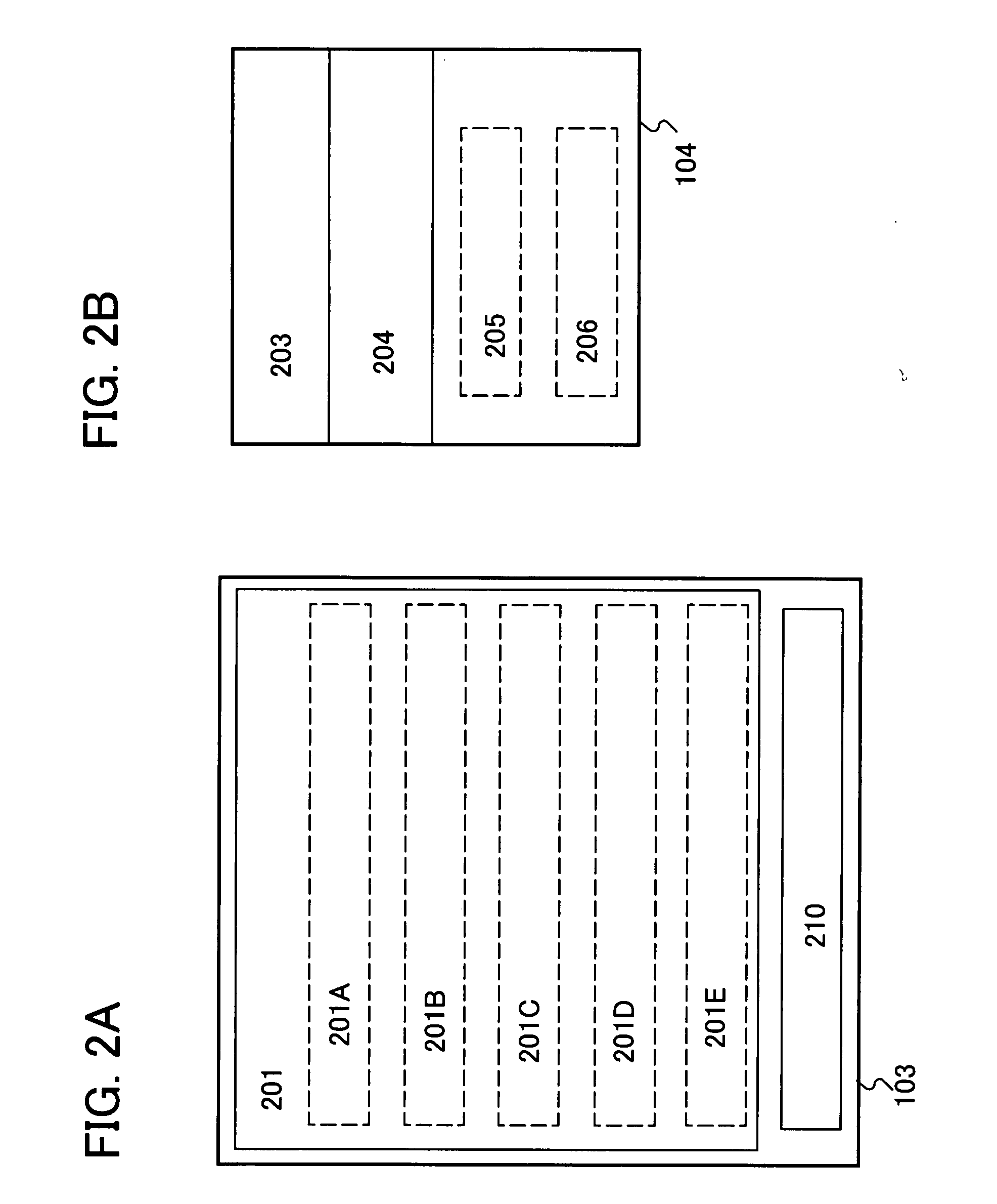
[0122]In this embodiment, applications of the invention and an example of a product which includes an application of the inve...


PUM


Abstract

To provide a semiconductor device in which power consumption at the time of an anti-collision operation is reduced. A semiconductor device includes an arithmetic circuit, a storage device, and circuits for transmitting and receiving signals to and from the outside. The arithmetic circuit includes a central processing unit and a controller. The central processing unit executes a program for using the controller to reduce power consumption when a signal is transmitted to the outside. The program has a structure which includes a plurality of routines. Representatively, the program includes a command determination routine, a UID value processing routine, a mask value comparison routine, an N-slot power consumption reduction routine, an N-slot counter routine, and the like.

Description

BACKGROUND OF THE INVENTION[0001]1. Field of the Invention[0002]The present invention relates to semiconductor devices. In particular, the present invention relates to semiconductor devices which transmit and receive signals to and from the outside, or so-called IC chips (also referred to as ID chips, IC tags, ID tags, RF tags, wireless tags, electronic tags, or transponders) for RFID (radio frequency identification).[0003]Note that in this specification, a semiconductor device refers to any device which can function by utilizing a semiconductor property.[0004]2. Description of the Related Art[0005]Due to the development of computer technology and improvement of image recognition technology, information identification using a medium such as a barcode has become widespread, and is used for identifying product data or the like. It is expected that the amount of information to be identified will further increase in the future. Meanwhile, information reading and the like using a barcode...

Claims


Application Information

Patent Timeline
Patent Type & Authority Applications(United States)
IPC IPC(8): G11C11/24
CPCG06K19/0707Y02B60/1221G06F1/3287G06F1/3203Y02B60/1282G06F1/3237G06K7/10019G06K19/07749G06K19/0712Y02B60/1278Y02D10/00G06K19/07
Inventor DEMBO, HIROKI
Owner SEMICON ENERGY LAB CO LTD
Why Eureka
Try Eureka