Method For Manufacturing Semiconductor Device Having Bulb-Type Recessed Channel

a semiconductor device and recessed channel technology, applied in the field of semiconductor devices, can solve the problems of reducing the size of transistors, reducing the threshold voltage and refresh property of cells, and unable to ensure stable operation of transistors, so as to improve the refresh properties and cell current characteristics, and increase the effective channel length

Active Publication Date: 2008-07-03
SK HYNIX INC
View PDF12 Cites 11 Cited by
  • Summary
  • Abstract
  • Description
  • Claims
  • Application Information

AI Technical Summary

Benefits of technology

[0007]The invention provides a method for manufacturing a semiconductor device having bulb-type recessed channels that forms a semiconductor device having advantages of FinFET structure and bulb-type recessed channels to increase the effective channel length thereby improving refresh properties and cell current characteristics.

Problems solved by technology

With a drastic decrease in the design rules for integrated circuit semiconductor devices, there has been difficulty in ensuring stable operation of transistors.
Especially, with a decrease in the design rules for semiconductor devices to a level of 70 nm or less, the size of transistors also has decreased so that the margin of the cell threshold voltage and refresh property reached its limitation.
However, commercialized high speed double data rate (DDR) 2 DRAM products define test conditions at a high temperature such that the data retention time decreases rapidly compared with the conventional DDR DRAM product.
Moreover, deterioration in the transistor drive current characteristics due to the reduced size of active regions in the width direction was also induced.
When the volume of the word line increases, the coupling capacitance between the word lines increases greatly thereby inducing a signal delay of the word line.
Thus, the refresh property may deteriorate due to increased leakage current.

Method used


Image

  • Method For Manufacturing Semiconductor Device Having Bulb-Type Recessed Channel
  • Method For Manufacturing Semiconductor Device Having Bulb-Type Recessed Channel
  • Method For Manufacturing Semiconductor Device Having Bulb-Type Recessed Channel

Examples


Embodiment Construction

[0019]Preferred embodiments of the invention will now be described in detail with reference to the accompanying drawings. However, various variations and modifications can be made in the embodiments and the invention is not to be construed as limited to the following embodiments. The thickness has been magnified to clearly illustrate a plurality of layers and regions in the drawing. The same numerical symbols have been given to the similar parts throughout the specification.

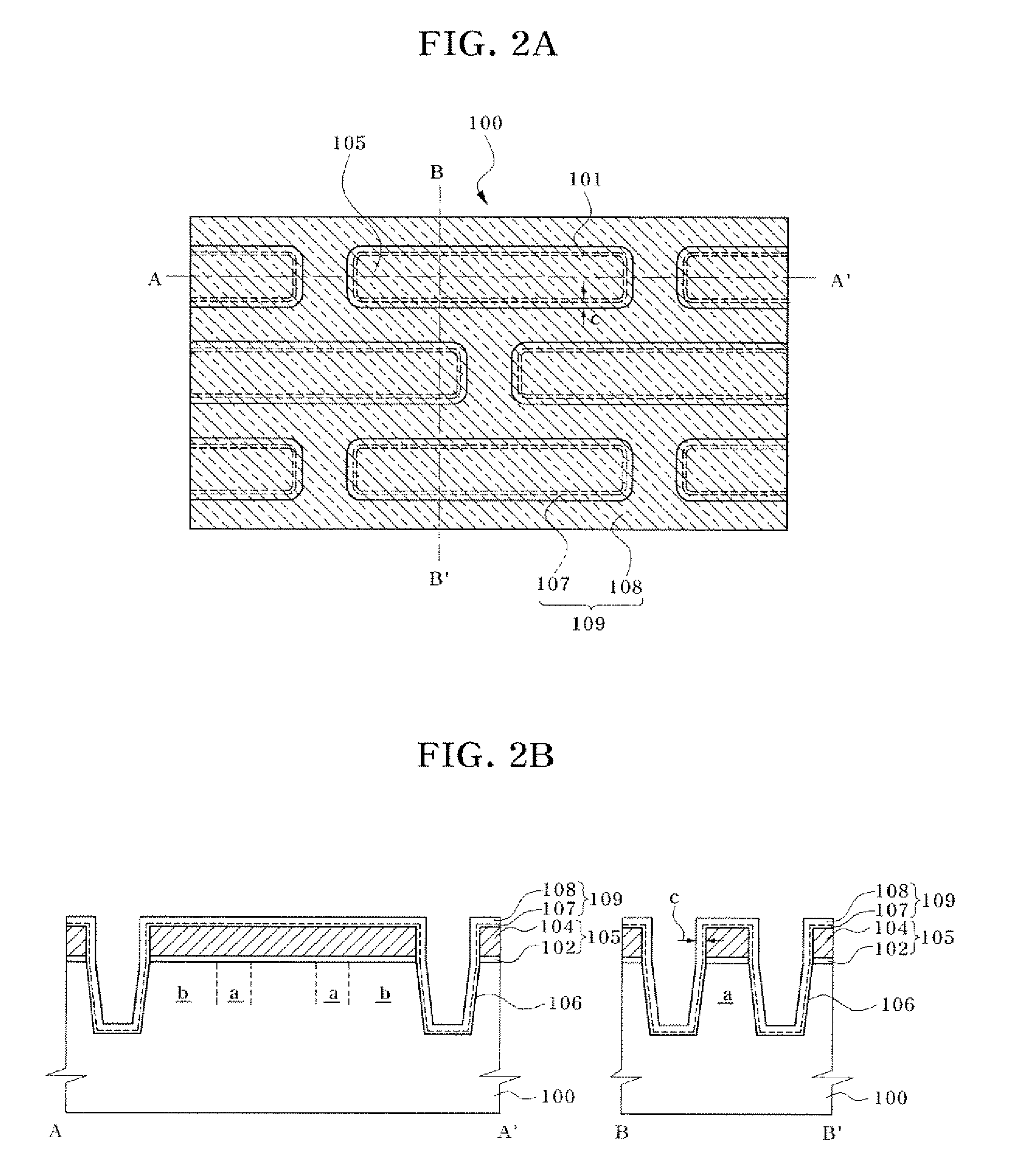
[0020]FIGS. 1A to 11B are diagrams illustrating a method for manufacturing a semiconductor device having bulb-type recessed channels according to an embodiment of the invention.

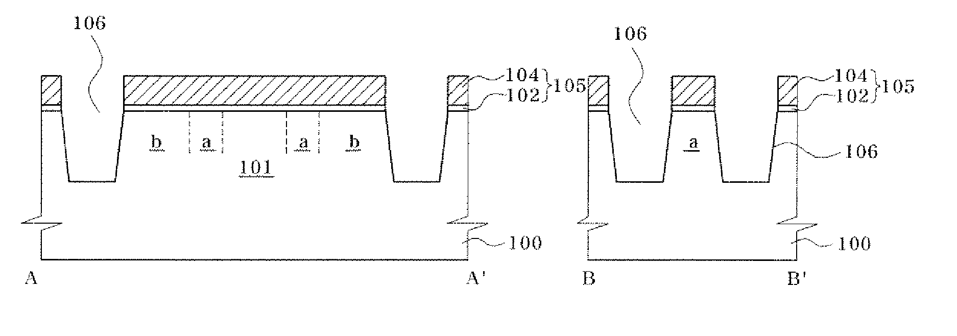
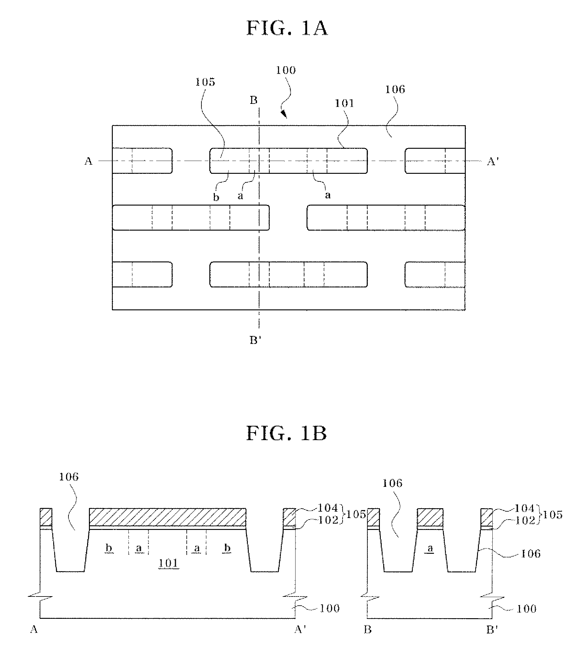
[0021]Referring to FIGS. 1A and 1B, a trench 106 for device isolation is formed in a semiconductor substrate 100. Here, FIG. 1B is a part of a cross-sectional view along in the direction of A-A′ and B-B′ of FIG. 1A. Hereinafter, description thereof will be omitted.

[0022]Specifically, a pad oxide layer and pad nitride layer are sequentially...


PUM


Abstract

A method for manufacturing a semiconductor device having a bulb-type recessed channel including: forming a trench that defines an active region including a channel region having a sidewall and a junction region in a semiconductor substrate; forming a device isolation layer that buries the trench, and forming a sidewall pattern that covers the sidewall of the channel region; forming a bulb-type trench by overlapping with the channel region in the semiconductor substrate, and forming a bottom protrusion having a predetermined space parted from the device isolation layer by removing the sidewall pattern; and forming a gate stack that overlaps with the bulb-type trench and the bottom protrusion.

Description

CROSS-REFERENCE TO RELATED APPLICATION[0001]The priority of Korean patent application number 10-2006-138808, filed on Dec. 29, 2006, which is incorporated by reference in its entirety, is claimed.BACKGROUND OF THE INVENTION[0002]The invention relates to a semiconductor device and, more particularly, to a method for manufacturing a semiconductor device having bulb-type recessed channels.[0003]With a drastic decrease in the design rules for integrated circuit semiconductor devices, there has been difficulty in ensuring stable operation of transistors. Especially, with a decrease in the design rules for semiconductor devices to a level of 70 nm or less, the size of transistors also has decreased so that the margin of the cell threshold voltage and refresh property reached its limitation.[0004]Under such circumstances, a great deal of research has been conducted on methods for ensuring a longer effective channel length without any increase in the design rules. Among the methods for ensu...

Claims


Application Information

Patent Timeline
Patent Type & Authority Applications(United States)
IPC IPC(8): H01L21/336
CPCH01L29/66621H01L29/7851H01L29/66795H01L21/18
Inventor LEE, JIN YUL
Owner SK HYNIX INC
Why Eureka
Try Eureka