Method, system, and computer program product for determining three-dimensional feature characteristics in electronic designs

a technology of electronic designs and feature characteristics, applied in the field of three-dimensional feature characteristics determination of computer program products, can solve the problems of increasing the r-c time constant, increasing the delay caused by the increased r-c time constant, and aggravate the electro-migration problem by using low-k dielectric materials

Active Publication Date: 2008-07-03
CADENCE DESIGN SYST INC
View PDF5 Cites 33 Cited by
  • Summary
  • Abstract
  • Description
  • Claims
  • Application Information

AI Technical Summary

Benefits of technology

[0008]As a result, there exists a need for a more accurate and effective method for predicting the profile of the features so as to more accurately determine the properties of the features and thus more effectively determine whether the design in fact meet the manufacturability, performance, reliability, and / or other design objectives. The present invention is directed to an improved method, system, and computer program product for an electronic design automation tool to more accurately determine the three-dimensional profiles of features in an electronic design. Some embodiments utilizes the above method, system, and / or computer program to produce more accurate wire / feature profiles for determine whether the design meets certain design objectives.

Problems solved by technology

As the devices shrinks smaller, the delay caused by the increased R-C time constant becomes more significant over the delay caused by the actual profiles of the features.
However, the use of low-k dielectric material aggravates the electro-migration problem due to the poor thermal conductivity of these low-k dielectric materials.
However, even these more advanced approaches only consider the wire properties as a function of a few characteristics, such as the width of a wire and the distance to the nearest neighbors.
Although these assumptions arose out of practical considerations and have worked while the thickness variation is relatively insignificant as compared to the geometry sizes, such an assumption appears to be outdated, especially in light of the current development in incorporating the topological variations of each film into the electronic designs and the continuously shrinkage in sizes of device features.
Moreover, wire width cannot be arbitrarily changed due to the polycrystalline structure of the interconnect materials.
Nonetheless, the above rule-based methods pose new problems.
For instance, a good interconnect may be wrongfully determined to be improper for failing to meet certain design rules or for producing unacceptable R-C delay even though the interconnect actually satisfies the design goals by having certain thickness that is different from the assumed value.
A contrary example is that a bad interconnect may also be wrongfully determined to be proper for meeting the metal density rules and / or the delay requirement.
Additionally, the continual effort to scale down to the deep submicron region renders the design more susceptible to even slight variations of or deviations of the design features from their true profile particularly in deep submicron designs.
Furthermore, using presumed thicknesses of certain features or thickness information from the process / fabrication models without truthfully approximating the true profiles of certain features would sometimes falsely identify a perfectly good design to be bad and a bad design to be good.
In some other times, using presumed thicknesses or cross sections of certain features or thickness information from the process / fabrication models without truthfully approximating the true profiles of certain features would falsely report that certain designs fail to meet certain objectives and cause unnecessary redesign or waste of valuable real estate in the chip area.

Method used


Image

  • Method, system, and computer program product for determining three-dimensional feature characteristics in electronic designs
  • Method, system, and computer program product for determining three-dimensional feature characteristics in electronic designs
  • Method, system, and computer program product for determining three-dimensional feature characteristics in electronic designs

Examples


Embodiment Construction

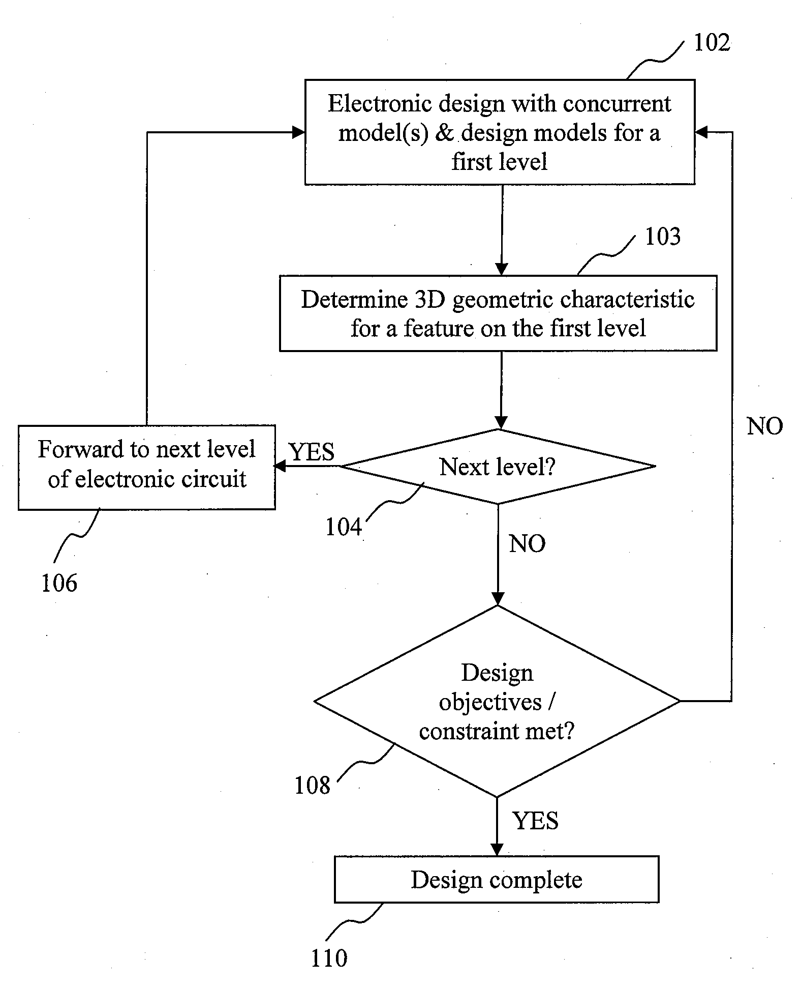
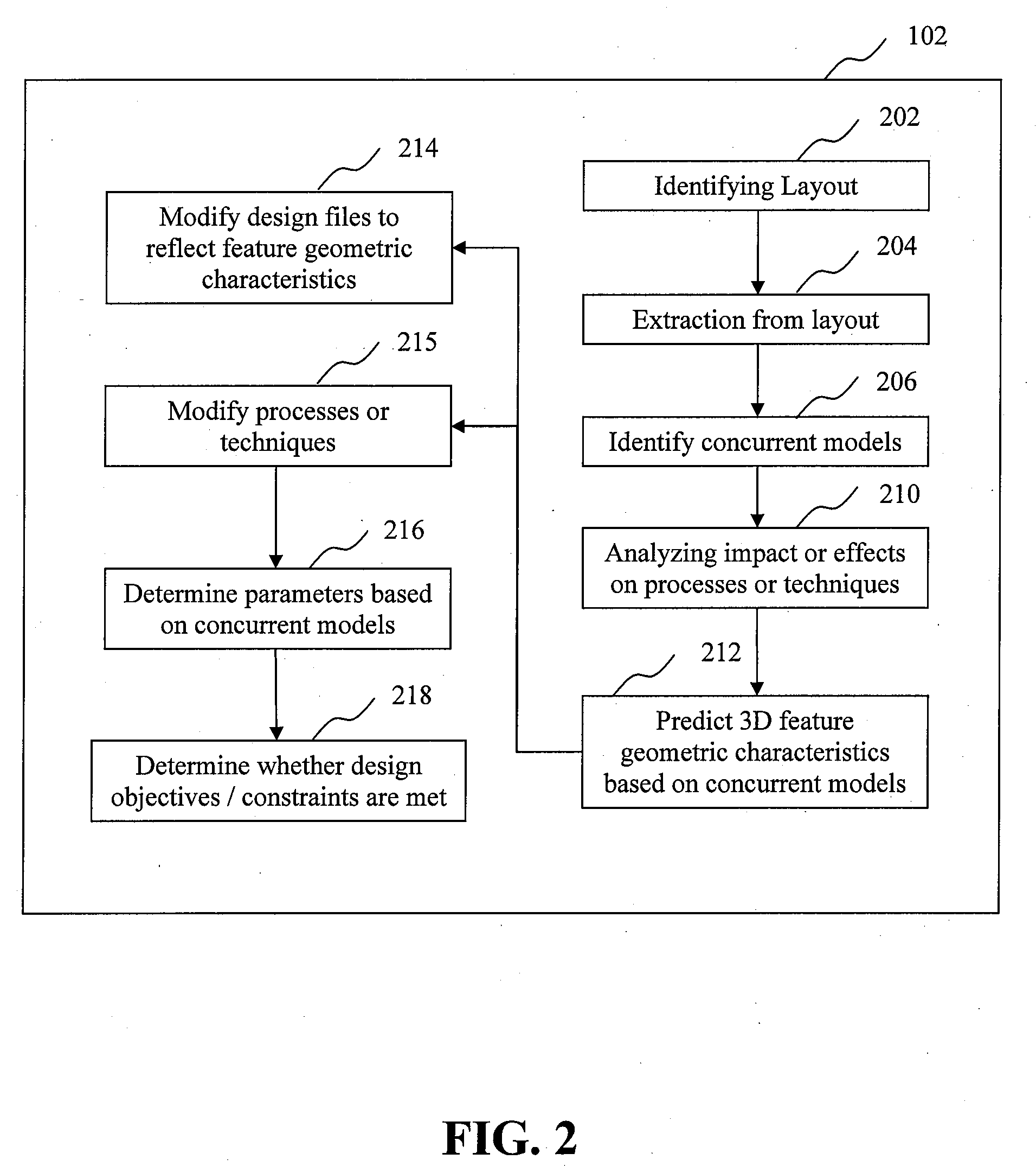
[0016]The present invention is directed to an improved method, system, and computer program product for an electronic design automation tool to more accurately determine the three-dimensional profiles of features in an electronic design. Some embodiments utilizes the above method, system, and / or computer program to produce more accurate wire / feature profiles for determine whether the design meets certain design objectives. As noted above, conventional methods and systems assume a thickness value for each wire and neglect the impact of variation of wire properties as a result of deviation from the assumed rectangular profile and thus either use unnecessary computation resources to produce the results or even produce unsatisfactory results. More details concerning the concurrent models are disclosed in U.S. application Ser. No. ______ under Attorney Docket No. CA7052682001 and application Ser. No. ______ under Attorney Docket No. CA7052692001, both of which are filed concurrently with...


PUM


Abstract

Disclosed are an improved method, system, and computer program product for a method or system with concurrent models to more accurately determine and represent the three-dimensional design features of electronic designs. Some embodiments disclose a method or a system for determining the design feature characteristics based upon their respective three-dimensional profiles. Some other embodiments further determine whether the design objectives or constraints are met or may be relaxed based upon the design feature characteristics in order to complete the design. Other embodiments store the profile or geometric characteristics, or information derived therefrom, in a database associated with the design to reduce the need for potentially expensive computations. The method or system may modify the designs or the processes to reflect whether the design objectives or constraints are met or relaxed.

Description

CROSS-REFERENCE TO RELATED APPLICATION(S)[0001]This application claims the benefit of U.S. Provisional Application No. 60 / 877,941, filed on Dec. 29, 2006, which is hereby incorporated by reference in its entirety.BACKGROUND OF THE INVENTION[0002]As the device size shrinks, especially into the deep-submicron regime, and clock frequency increases, the electrical properties of circuit design features become more prominent, and chips are more susceptive to breakdown during fabrication due to, for example, antenna effect or to wear out over time due to, for example, electro-migration.[0003]One approach assumes the thickness of certain features, such as the features or interconnects, to be a certain numeric value and manipulates the widths and / or lengths of such features to achieve the design objectives. Another approach obtains the thickness of the features from process model and / or fabrication information and use such information together with the width and / or length information to more...

Claims


Application Information

Patent Timeline
Patent Type & Authority Applications(United States)
IPC IPC(8): G06F17/50
CPCG06F17/5081G06F30/398
Inventor WHITE, DAVIDSCHEFFER, LOUIS K.
Owner CADENCE DESIGN SYST INC
Why Eureka
Try Eureka