

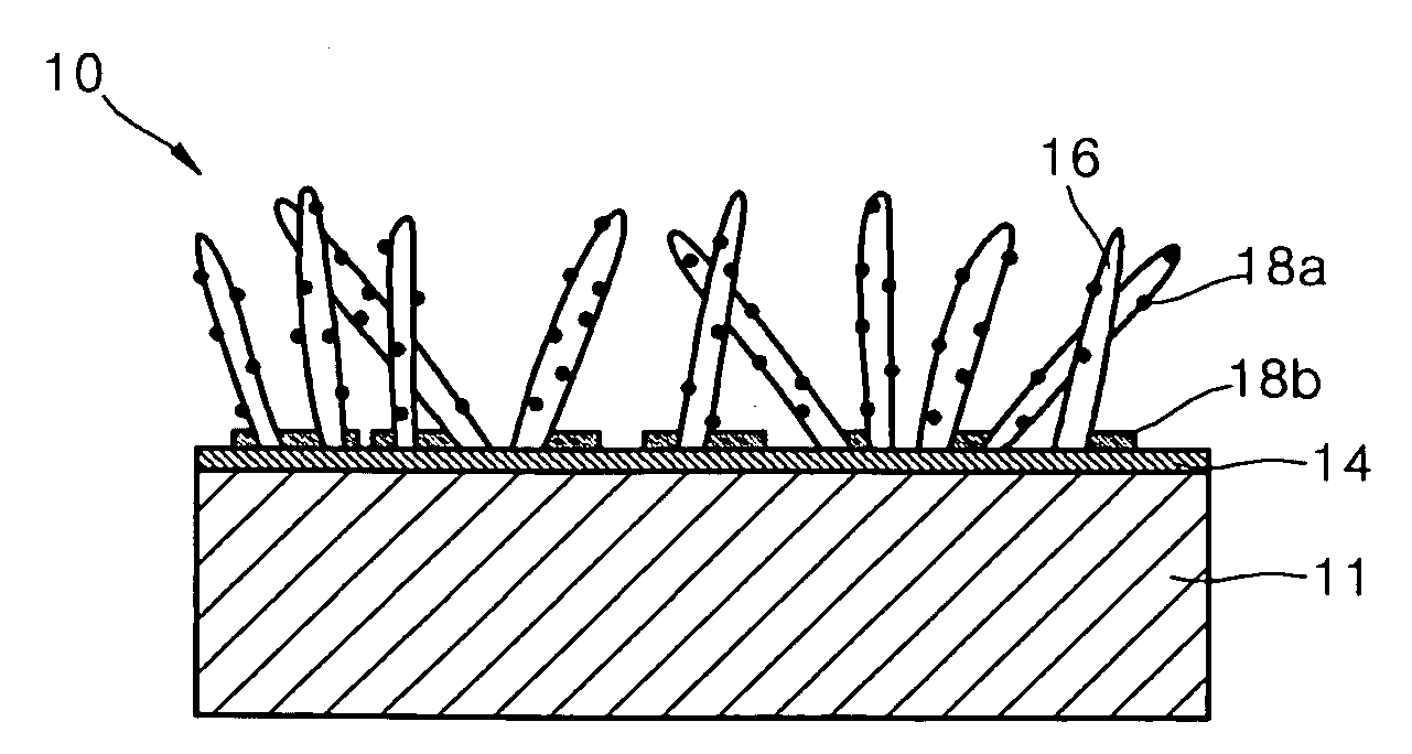
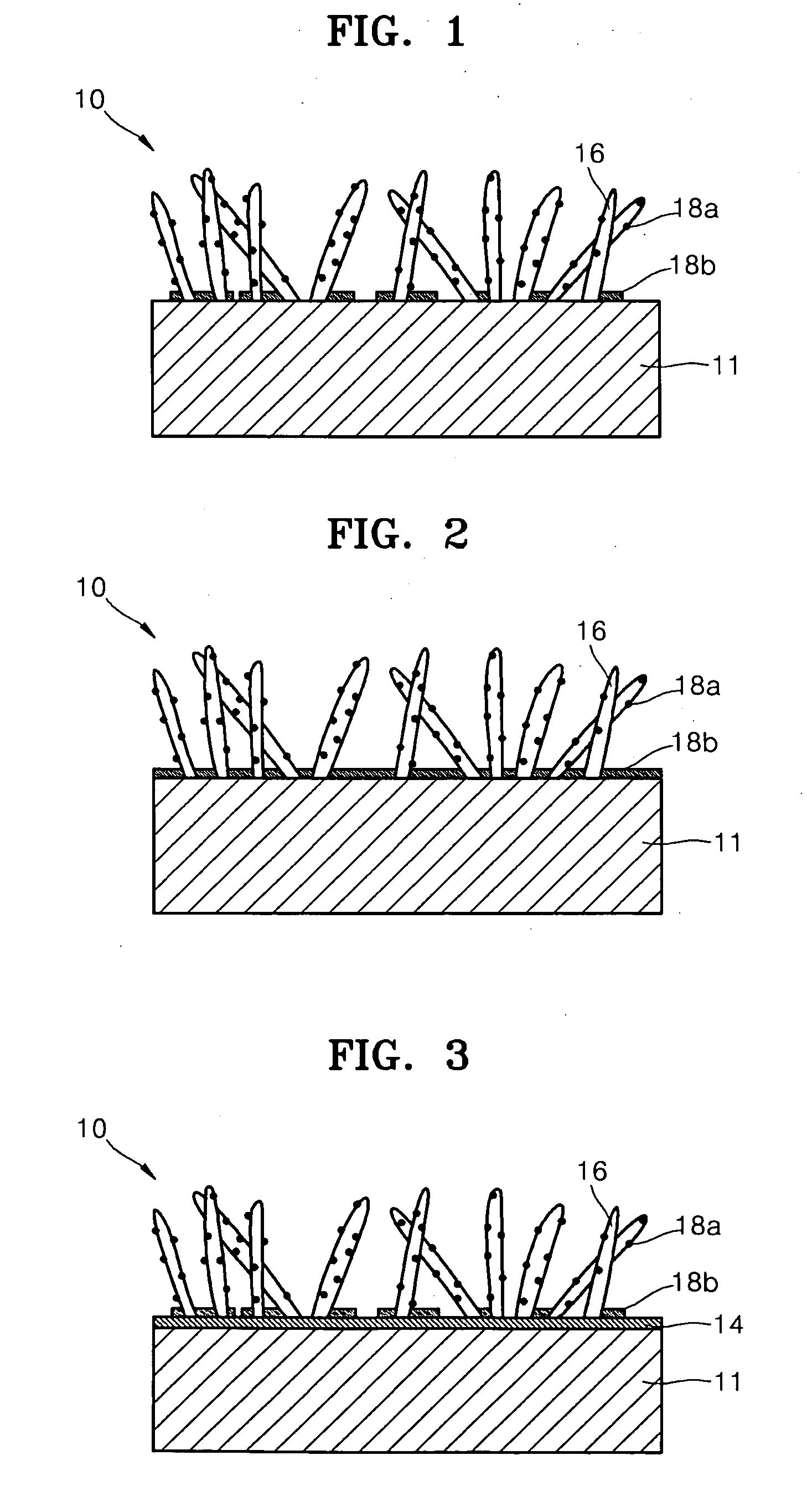
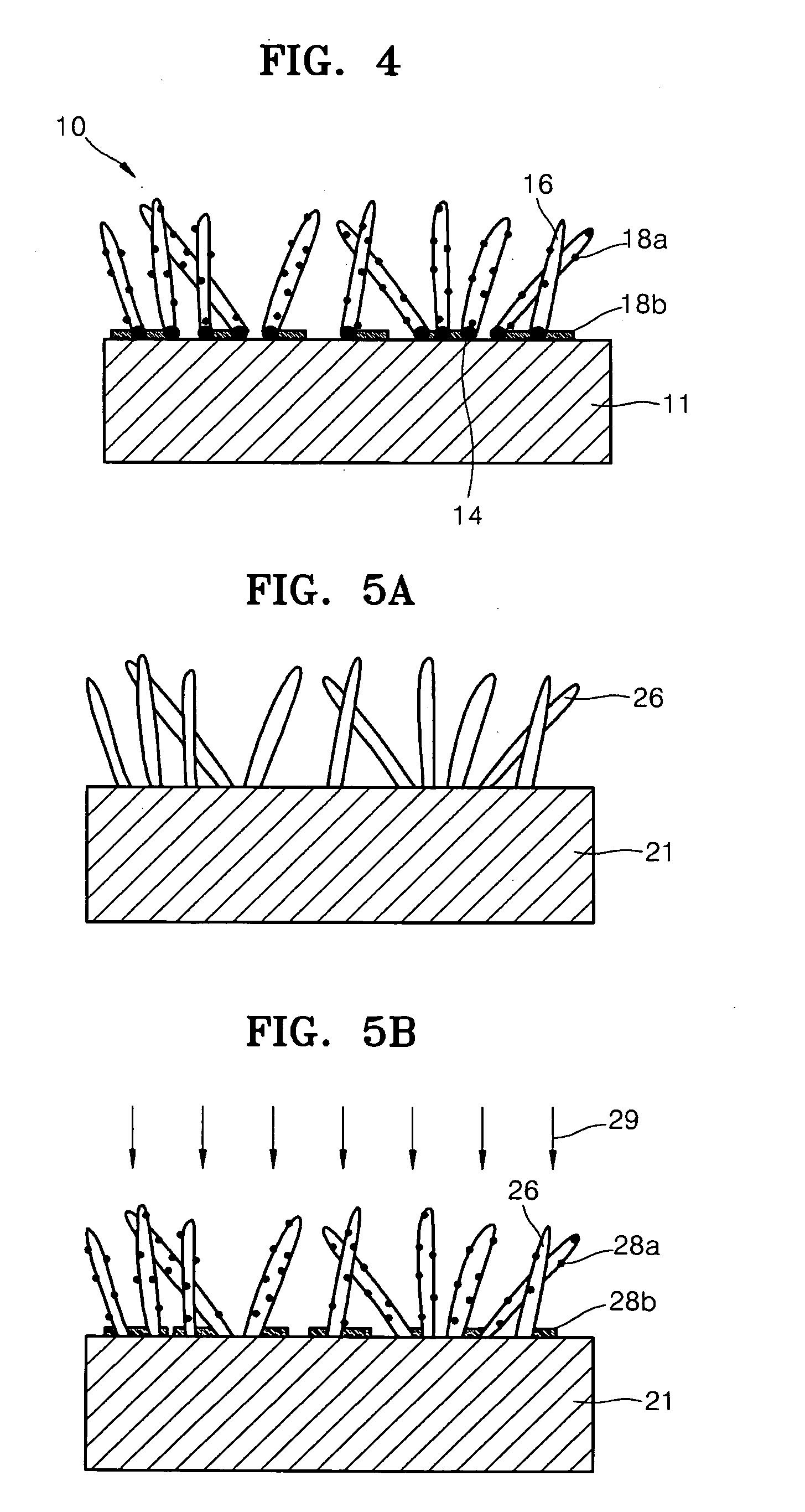
Field emission electrode, method of manufacturing the same, and field emission device comprising the same
- Summary
- Abstract
- Description
- Claims
- Application Information
AI Technical Summary
Benefits of technology
Problems solved by technology
Method used
Image

Examples
example
a) Synthesis of Single-Wall Carbon Nanotubes (SWNTs)
[0081]To allow observation by transmission electron microscopy, a copper grid was provided and a solution containing catalyst particles (an aqueous solution containing iron nitrate, bis(acetylacetonate)dioxomolybdenum, and alumina nanoparticles) for growing carbon nanotubes were spin coated on the copper grid to form a catalytic layer for growing carbon nanotubes. Then, the coated grid was placed into a vacuum chamber of a plasma CVD apparatus (a remote plasma enhanced CVD apparatus), and a H2O plasma discharge was generated to grow carbon nanotubes. Growth conditions of the carbon nanotubes are described in Table 1.
TABLE 1Temperature in vacuum chamber450° C.Pressure in vacuum chamber0.37 torrH2O Plasma power15 WSource gasCH4(introduced together with water)Flow rate of source gas60 sccmSynthesis time of carbon nanotubes180 sec
[0082]FIGS. 7A through 7C illustrate transmission electron microscope (TEM) images, taken at different magn...
PUM
 Abstract
Description
Claims
Application Information