Organic el element and organic light-emitting device

Inactive Publication Date: 2012-08-23
MITSUBISHI CHEM CORP
View PDF6 Cites 14 Cited by
  • Summary
  • Abstract
  • Description
  • Claims
  • Application Information

AI Technical Summary

Benefits of technology

[0040]The organic light-emitting device of the present invention has a constantly long life and is capable of suppressing an increase of the voltage with any one of red-, green- and blue-elements.
[0041]Further, the organic EL element of the present invent

Problems solved by technology

However, conventional organic EL elements employing phosphorescence molecules were practically insufficient with respect to the driving stability although providing emissions with high efficiency, and it has been difficult to realize a display device having high efficiency and long life.
In vapor deposition by means of a shadow mask, along with the trend for a large screen of a substrate, the corresponding enlargement of a metal mask brings about problems such as deficiency in the pattern precision, deficiency in the pattern-positioning precision, etc.
Further, at the time of such patterning, problems such as a decrease in the yield due to particles to be generated, an increase of the cost due to such an yield decrease, etc., are conceivable.
Thus, the vacuum deposition employing a shadow mask has a problem that it is disadvantageous for mass production or large size modification.
BCP makes it possible to obtain very good efficiency when applied to a phosphorescence organic EL element (Non-Patent Document 1), but is accompanied by such a drawback that the life of an organic EL element containing BCP is substantially limited. T. Tsutsui et al (Non-Patent Document 2) have pointed o

Method used


Image

  • Organic el element and organic light-emitting device
  • Organic el element and organic light-emitting device
  • Organic el element and organic light-emitting device

Examples


Example

Reference Example 1

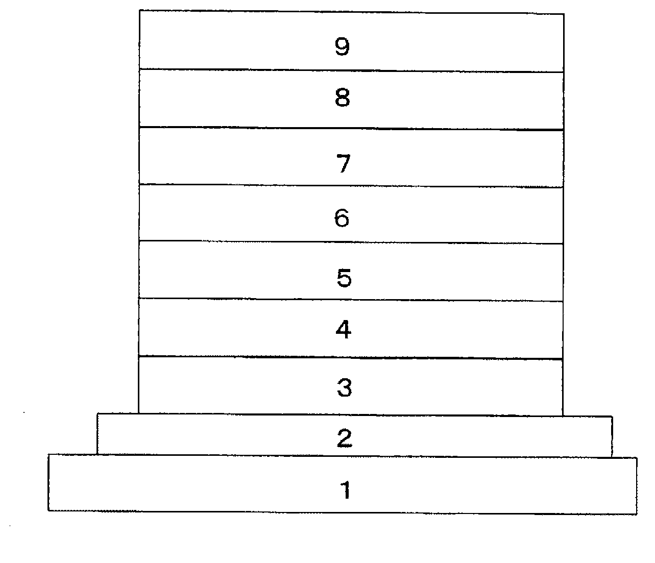
[0287]An organic EL element having the structure shown in FIG. 1 was prepared by the following method.

(Preparation of ITO Substrate)

[0288]An indium.tin oxide (ITO) transparent conductive film deposited in a thickness of 150 nm on a glass substrate 1 (a sputter-deposited product, sheet resistance: 15Ω) was subjected to patterning in stripes with a width of 2 mm by means of a usual photolithography technique and hydrochloric acid etching to form an anode 2.

(Pre-Treatment)

[0289]The substrate having the anode patterned as described above (ITO substrate) was subjected to cleaning in the order of ultrasonic cleaning by a surfactant, water washing by pure water and ultrasonic cleaning by isopropyl alcohol, then dried by compressed air and finally subjected to ultraviolet ray ozone cleaning for 1 minute.

(Film Formation of Hole Injection Layer)

[0290]Then, a hole injection layer 3 was formed by a wet film-forming method as follows. As the material for the hole injection lay...

Example

Reference Example 2

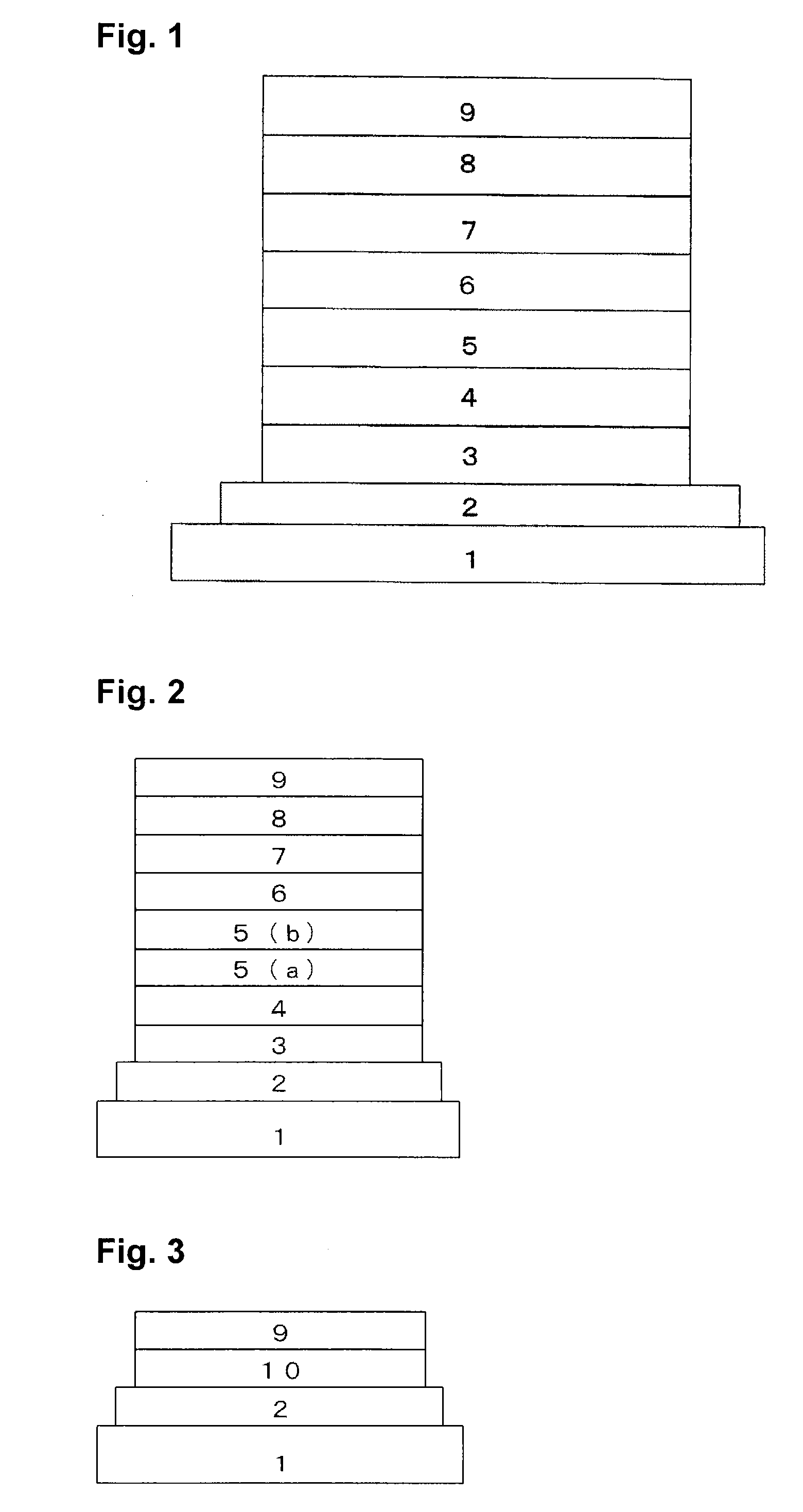
[0303]An organic EL element was prepared in the same manner as in Reference Example 1 except that in Reference Example 1, the hole-relaxing material HA-1 was changed to the following BAlq as a hole-blocking material.

Example

Reference Example 3

[0304]An organic EL element was prepared in the same manner as in Reference Example 1 except that in Reference Example 1, the hole-relaxing material HA-1 was changed to the following HB-1 as a hole-blocking material.

[Results]

[0305]With respect to the organic EL elements obtained in Reference Examples 1, 2 and 3, respectively, the luminance half-time as measured by the following method is shown in the following Table 1.

[Measuring Method]

[0306]The method for measuring the luminance half-time was carried out by observing by a photodiode a change in luminance when a voltage at which the luminance became 2,000 nit (only green element: 4,000 nit) when a DC constant current was applied to the prepared organic EL element during the test, whereby the time (luminance half-time) until the luminance value became a half of the value at the initiation of the test, i.e. 1,000 nit (only green element: 2,000 nit) was obtained. The current applying test was carried out in a room wh...


PUM

PropertyMeasurementUnit
Electric field strengthaaaaaaaaaa
Efficiencyaaaaaaaaaa
Electron mobilityaaaaaaaaaa

Abstract

To provide an organic EL element having high efficiency and long life, without accumulating holes at the interface between a light-emitting layer and a layer on the cathode side, and an organic light-emitting device.
An organic EL element having a light-emitting layer between an anode and a cathode, wherein the light-emitting layer contains a light-emitting material and a charge-transporting material, the element has a hole relaxation layer adjacent to the cathode side of the light-emitting layer, the hole relaxation layer contains a hole-relaxing material, the hole-relaxing material is an organic compound having a hole-transporting unit and an electron-transporting unit, and at least one type of the charge-transporting material and at least one type of the hole-relaxing material are the same organic compound; and an organic light-emitting device containing such an element.

Description

TECHNICAL FIELD[0001]The present invention relates to an organic EL element having high efficiency and long life, and an organic light-emitting device having such an element.BACKGROUND ART[0002]For the purpose of increasing luminous efficiency of an organic EL element, an element employing phosphorescence (emission by triplet excitons) instead of fluorescence (emission by singlet excitons) is being studied. By employing phosphorescence, the efficiency is considered to be improved about three times as compared with an element employing fluorescence, and it has been reported to use a europium complex, a platinum complex or the like as phosphorescence molecules. However, conventional organic EL elements employing phosphorescence molecules were practically insufficient with respect to the driving stability although providing emissions with high efficiency, and it has been difficult to realize a display device having high efficiency and long life.[0003]In an organic EL element, emission ...

Claims


Application Information

Patent Timeline
IPC IPC(8): H01L51/54
CPCH01L51/0039H05B33/22H01L51/0054H01L51/0058H01L51/0061H01L51/0067H01L51/0072H01L51/0081H01L51/0085H01L51/50H01L51/5036H01L51/504H01L51/5068H01L2251/55H01L51/0043H10K85/115H10K85/151H10K85/622H10K85/626H10K85/636H10K85/654H10K85/324H10K85/342H10K85/6572H10K50/00H10K50/125H10K50/13H10K50/157H10K2101/00
Inventor IMADA, ICHIROGOROHMARU, HIDEKITAKAHASHI, ATSUSHI
Owner MITSUBISHI CHEM CORP
Why Eureka
Try Eureka