
Electrophotographic photoconductor and image-forming apparatus

a photoconductor and photoconductor technology, applied in the field of electrophotoconductor and image-forming apparatus, can solve the problems of poor plasticity of the layer, difficulty in forming the photosensitive layer, and inorganic photoconductor, and achieve high charge potential, high reliability, and high sensitivity.

Active Publication Date: 2008-07-10
SHARP KK
View PDF1 Cites 10 Cited by
  • Summary
  • Abstract
  • Description
  • Claims
  • Application Information

AI Technical Summary

Benefits of technology

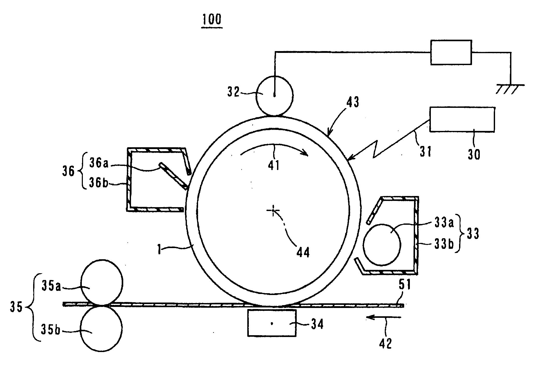
[0023]An object of the present invention is to provide a highly reliable electrophotographic photoconductor whose properties, such as charge potential, sensitivity, photoresponsiveness and charge-transportability, are not deteriorated even when used under low temperature environments or in a high-speed process, by using an organic photoconductive material having high charge potential, high sensitivity, sufficient photoresponsiveness, and high charge-transportability.

Problems solved by technology

Although having basic properties for an electrophotographic photoconductor to some degree, an inorganic photoconductor has problems of difficulties in forming its photosensitive layer, poor plasticity of the layer, high production costs, and the like.
In addition, generally inorganic photoconductive materials are so toxic that they are limited in terms of production and handling.
This is because conventional charge-transporting materials have low charge-transportability and therefore the charge-transportability of the charge-transport layer further decreases when the charge-transporting material content decreases as a result of the increase of the binder resin content.
If the photoresponsiveness of a photoconductor is poor, its residual surface potential increases and therefore the photoconductor is repeatedly used without sufficiently attenuating the surface potential.
In the photoconductor, the surface charge in the area exposed to light is not sufficiently erased, resulting in a rapid deterioration in image quality.
However, these compounds decrease in sensitivity under low temperature environments.

Method used


Image

  • Electrophotographic photoconductor and image-forming apparatus
  • Electrophotographic photoconductor and image-forming apparatus
  • Electrophotographic photoconductor and image-forming apparatus

Examples


production example 1

Productions of Exemplified Compound No. 1

[0189]From N,N′-diphenylbenzidine and diphenylacetaldehyde, an enamine compound represented by the following formula (7) was synthesized according to the method described in Japanese Patent Publication No. Hei 6 (1994)-348045-A, the disclosure of which is incorporated herein in its entirety by reference for any and all purposes:

[0190]Phosphorus oxychloride in an amount of 5.52 g (1.2 mole equivalents) was gradually added to 100 ml of ice-cold anhydrous N,N-dimethylformamide (DMF) and stirred for about 30 minutes to prepare a Vilsmeier reagent. To the ice-cold Vilsmeier reagent, 20.79 g (1.0 mole equivalent) of the enamine compound was gradually added. Then, the mixture was gradually heated up to 80° C., and stirred for 6 hours while kept at 80-90° C. After completion of the reaction, the mixture was left to cool, and then gradually added to 800 ml of a cold 4 N aqueous sodium hydroxide solution to precipitate the reaction product. The precipi...

production example 2

Production of Exemplified Compound No. 24

[0206]From N,N′-dinaphtyl-3,3′-dimethylbenzidine and diphenylacetaldehyde, an enamine compound represented by the following formula (10) was synthesized according to the method described in Japanese Patent Publication No. Hei 6 (1994)-348045-A:

[0207]Starting from the enamine compound, an aldehyde compound was prepared as described in Production Example 1. The thus obtained aldehyde compound was subjected to LC-MS and element analyses. The analysis data (see below) confirmed that the obtained compound was Exemplified Compound No. 24.

[0208]LC-MS analysis data:

[0209]Purity: 99.2%

[0210]A peak observed at a position corresponding to an MW of 1084.9

[0211](Theoretical MW of the molecular ion [M]+ of Exemplified Compound No. 24: 1084.50)

[0212]Peaks due to the fragment ions observed at positions corresponding to the MWs close to following:[0213]the theoretical MW of 1069 of the fragment ion [M-Me]+, wherein a methyl group is eliminated;[0214]the theor...

production example 3

Production of Exemplified compound No. 3

[0224]From 1-(4-phenylaminophenyl)-4-phenylaminobenzofuran and diphenylacetaldehyde, an enamine compound represented by the following formula (11) was synthesized according to the method described in Japanese Patent Publication No. Hei 6 (1994)-348045-A:

[0225]Starting from the enamine compound, an aldehyde compound was prepared as described in Production Example 1. The thus obtained aldehyde compound was subjected to LC-MS and element analyses. The analysis data (see below) confirmed that the obtained compound was Exemplified compound No. 30.

[0226]LC-MS analysis data:

[0227]Purity: 98.7%

[0228]A peak observed at a position corresponding to an MW of 988.9 (Theoretical MW of the molecular ion [M]+ of Exemplified Compound No. 30: 988.44)

[0229]Peaks due to the fragment ions observed at positions corresponding to the MWs close to the following:[0230]the theoretical MW of 911 of the fragment ion [M-φ]+, wherein a benzene ring is eliminated;[0231]the t...


PUM


Abstract

The present invention provides an electrophotographic photoconductor comprising an electroconductive substrate and a photosensitive layer provided on the electroconductive substrate, wherein the photosensitive layer comprises a charge-generating material and a charge-transporting material, the charge-transporting material comprising a compound represented by the general formula (1):wherein Ar1 and Ar2 each independently represent an optionally-substituted arylene or bivalent heterocyclic group; Ar3 and Ar4 each independently represent a hydrogen atom, or an optionally-substituted aryl or monovalent heterocyclic group, but are not simultaneously hydrogen atoms; or Ar3 and Ar4 may be taken together to form an optionally-substituted bivalent cyclic hydrocarbon or heterocyclic group; and n is 0 or 1.

Description

CROSS-REFERENCE TO RELATED APPLICATION[0001]This application is related to Japanese Patent Application No. 2006-356818 filed on Dec. 29, 2006, whose priority is claimed under 35 USC §119, the disclosure of which is incorporated herein in its entirety by reference for any and all purposes.BACKGROUND OF THE INVENTION[0002]1. Field of the Invention[0003]The present invention relates to an electrophotographic photoconductor which comprises an organic compound with high charge transportability as a charge-transporting material, and to an image-forming apparatus comprising the same.[0004]2. Description of the Related Art[0005]Recently, organic photoconductive materials have been widely researched and developed. They have been used for electrophotographic photoconductors (also referred to simply as “photoconductors”), and are now beginning to be applied to electrostatic recording devices, sensor materials, organic electroluminescent (EL) devices, etc.[0006]Organic photoconductors, in which...

Claims


Application Information

Patent Timeline
IPC IPC(8): G03C1/73G03G15/00
CPCG03G5/0614G03G2215/00957G03G5/0672G03G5/0668G03G5/061443G03G5/061473G03G5/06149
Inventor OBATA, TAKATSUGUKONDOH, AKIHIRO
Owner SHARP KK
Learn More