Nanotopography control and optimization using feedback from warp data

a technology of warp data and nanotopography, applied in adaptive control, lapping machines, instruments, etc., can solve the problems of substantial yield loss, non-adjustment of topology degradation, and degradation of the topology of the wafer surface, so as to improve the nanotopography, less lag time, and less time

Active Publication Date: 2008-07-10
GLOBALWAFERS CO LTD
View PDF48 Cites 32 Cited by
  • Summary
  • Abstract
  • Description
  • Claims
  • Application Information

AI Technical Summary

Benefits of technology

[0008]Aspects of the invention permit nanotopography feedback in less time, allowing adjustments that can be made to improve nanotopography to be recognized and implemented with less lag time for improved quality control and / or wafer yield. According to one aspect of the invention, data indicative of a profile of a wafer ground using a double side grinder is used to predict a nanotopography of the ground wafer. A grinding parameter for improving the nanotopography of subsequently ground wafers is determined based on the predicted nanotopography. The operation of the double side grinder is adjusted in accordance with the determined grinding parameters. As such, aspects of the present invention provide improved nanotopography for wafers subsequently ground by the double side grinder. In another aspect, the present invention utilizes warp data to provide the nanotopography feedback. For example, the present invention may use warp data obtained from a warp measurement device generally used in wafer processing. As such, the present invention advantageously provides a cost-effective and convenient method for improving nanotopography.

Problems solved by technology

While this grinding process can improve flatness and / or parallelism of the ground wafer surfaces, it can cause degradation of the topology of the wafer surfaces.
Specifically, misalignment of the hydrostatic pad and grinding wheel clamping planes are known to cause such degradation.
Post-grinding polishing produces a highly reflective, mirrored wafer surface on the ground wafer but does not address topology degradation.
In particular, NT defects like C-Marks and B-Rings take form during grinding process from misalignment of the hydrostatic pad and grinding wheel clamping planes and may lead to substantial yield losses.
Unfortunately, the dynamics of the grinding operation and the effects of differential wear on the grinding wheels cause the planes to diverge from alignment after relatively few operations.
The alignment steps, which are highly time consuming when performed by an operator, must be repeated so often as to make it a commercially impractical way of controlling operation of the grinder.
Additionally, current techniques do not inform the operator of the particular adjustments that should be made to the clamping planes.
Accordingly, the manual alignments are inconsistent among operators and often fail to improve wafer nanotopography.
Further, there is usually some lag between the time that undesirable nanotopography features are introduced into a wafer by a double side grinder and the time they are discovered.
As such, undesirable nanotopography features introduced into the wafer by the double side grinder cannot be identified until post-polishing.
If suboptimal settings of the grinder cause an NT defect, then, it is likely that all the wafers in the cassette will have this defect leading to larger yield loss.
In addition to this unavoidable delay in conventional wafer processes, the operator must wait for each cassette to be processed before getting feedback from the measurements.
This leads to a considerable amount of down-time.
If the next cassette is already ground before receiving the feedback, there is a risk of even more yield loss in the next cassette due to improper grinder settings.

Method used


Image

  • Nanotopography control and optimization using feedback from warp data
  • Nanotopography control and optimization using feedback from warp data
  • Nanotopography control and optimization using feedback from warp data

Examples


Embodiment Construction

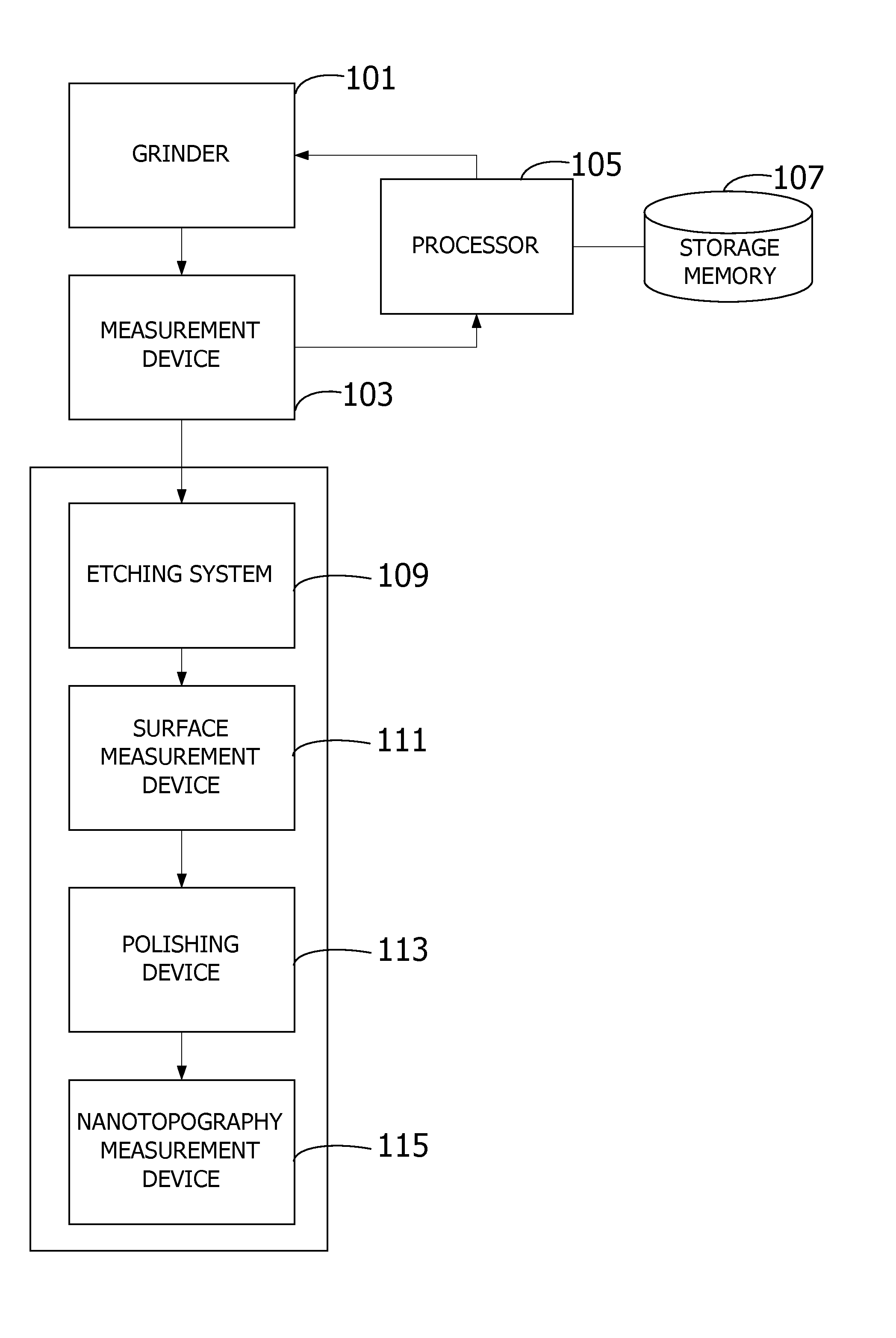
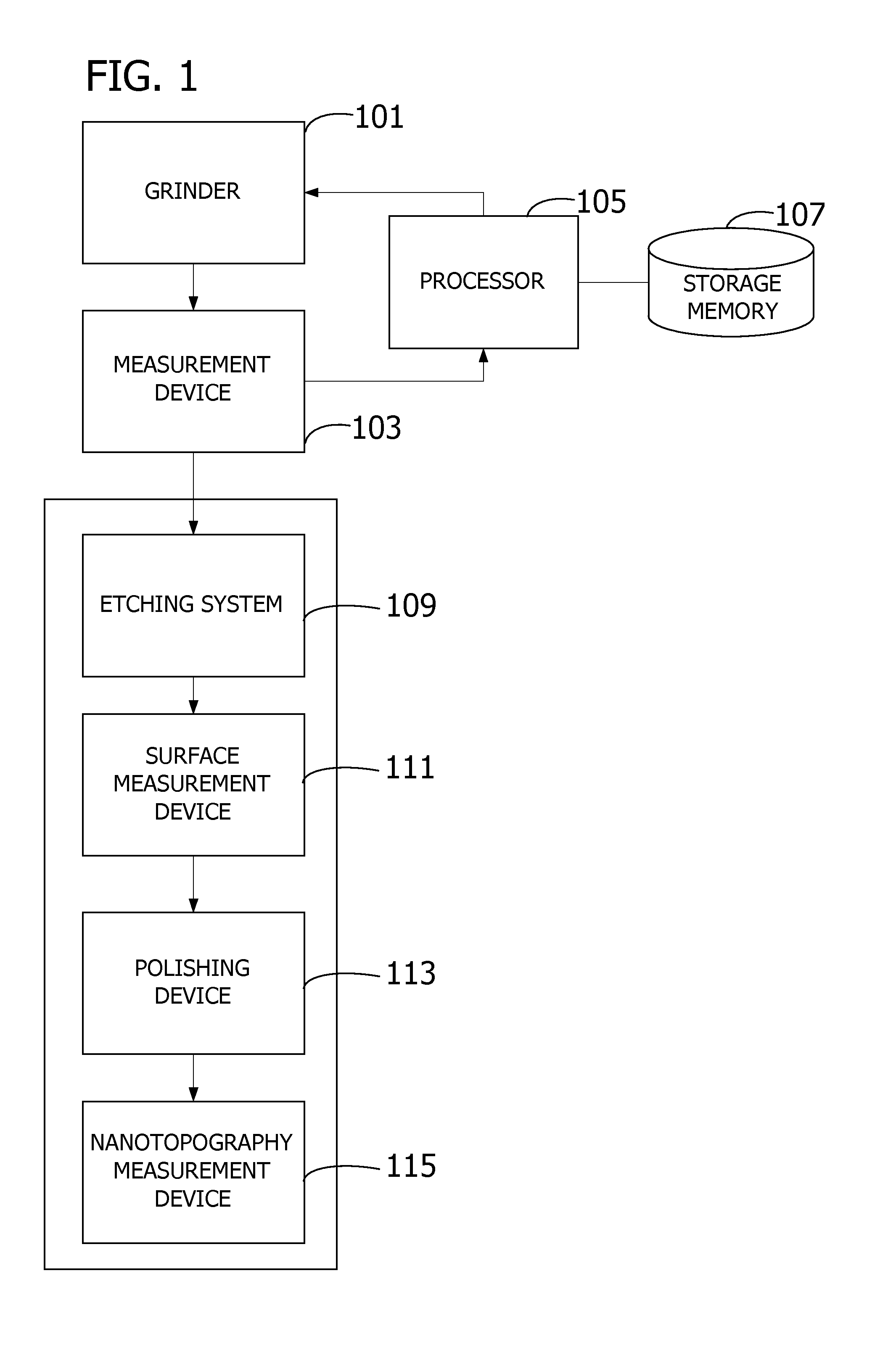
[0030]Referring now to the drawings, aspects of the invention permit nanotopography feedback in less time, allowing adjustments that can be made to improve nanotopography to be recognized and implemented with less lag time for improved quality control and / or wafer yield. In FIG. 1, a block diagram illustrates a system for processing a semiconductor wafer according to an embodiment of the present invention. For purposes of illustration and not limitation, the system includes a grinder 101, a measurement device 103, and a processor 105 having a storage memory 107 associated therewith. The grinder 101 grinds a wafer and the measurement device 103 measures data indicative of a profile of the ground wafer. The ground wafer at this point is unetched and unpolished. The processor 105 is configured to provide feedback for adjusting a grinding parameter based on the measured data. For example, one or more of the grinding wheels of grinder 101 may be moved in order to improve the nanotopograp...


PUM


Abstract

Processing a wafer using a double side grinder having a pair of grinding wheels. Warp data is obtained by a warp measurement device for measuring warp of a wafer as ground by the double side grinder. The warp data is received and a nanotopography of the wafer is predicted based on the received warp data. A grinding parameter is determined based on the predicted nanotopography of the wafer. Operation of the double side grinder is adjusted based on the determined grinding parameter.

Description

CROSS-REFERENCE TO RELATED APPLICATION[0001]This application is a continuation-in-part of co-pending U.S. patent application Ser. No. 11 / 617,430, filed Dec. 28, 2006, and of co-pending U.S. patent application Ser. No. 11 / 617,433, filed Dec. 28, 2006, both of which claim the benefit of U.S. Provisional Application No. 60 / 763,456, filed Jan. 30, 2006, the entire disclosures of which are incorporated herein by reference.BACKGROUND OF THE INVENTION[0002]Aspects of the invention relate generally to processing semiconductor wafers and more particularly to controlling and optimizing wafer nanotopography during processing.[0003]Semiconductor wafers are commonly used as substrates in the production of integrated circuit (IC) chips. Chip manufacturers require wafers that have extremely flat and parallel surfaces to ensure that a maximum number of chips can be fabricated from each wafer. After being sliced from an ingot, wafers typically undergo grinding and polishing processes designed to imp...

Claims


Application Information

Patent Timeline
Patent Type & Authority Applications(United States)
IPC IPC(8): B24B49/00
CPCB24B7/228B24B51/00B24B37/28B24B37/005
Inventor BHAGAVAT, SUMEET S.VANDAMME, ROLAND R.KOMURA, TOMOMIKANEKO, TOMOHIKOKAZAMA, TAKUTO
Owner GLOBALWAFERS CO LTD
Why Eureka
Try Eureka