Method for Analyzing Component Mounting Board

a technology for component mounting boards and physical properties, applied in error detection/correction, design optimization/simulation, instruments, etc., can solve problems such as malfunctions

Inactive Publication Date: 2008-07-10
GK BRIDGE 1
View PDF3 Cites 9 Cited by
  • Summary
  • Abstract
  • Description
  • Claims
  • Application Information

AI Technical Summary

Problems solved by technology

Specifically, there is possibility that the curvature beyond the limit will occur in a multilayer wiring board, and a malfunction will occur in the multilayer wiring board due to external force or temperature variation.

Method used


Image

  • Method for Analyzing Component Mounting Board
  • Method for Analyzing Component Mounting Board
  • Method for Analyzing Component Mounting Board

Examples


embodiment 1

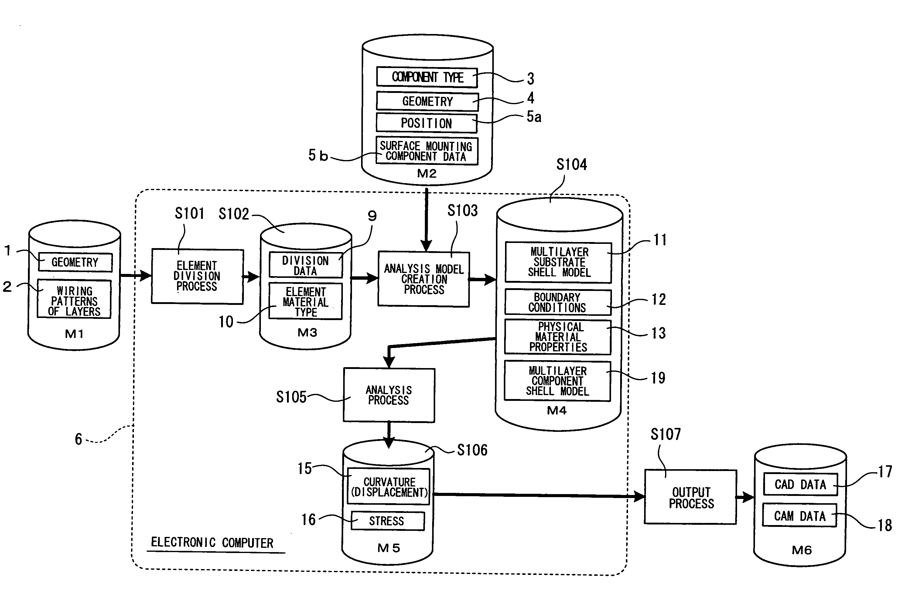
[0052]FIG. 1 shows a flow of stress analysis based on a method for analyzing a component mounting board.

[0053]When processing is initiated, an external geometry 1 of the multilayer wiring board to be analyzed and data 2 of a wiring pattern of each layer are prepared as a first file M1 and a component type 3, a geometry 4 and a position 5a are prepared as a second file M2 when a component is arranged inside the multilayer wiring substrate other than a wiring pattern, via hole, or the like in the multilayer wiring board. In terms of a component mounted to a surface of the multilayer wiring board, surface mounting component data 5b is prepared as the second file M2 for a mounting method, geometry and structure described for each component. In the geometry of the surface mounting component data 5b, data regarding an external geometry of a package and an arrangement of external connection terminals are included in the case of an integrated circuit. In terms of the structure, data regardi...

embodiment 2

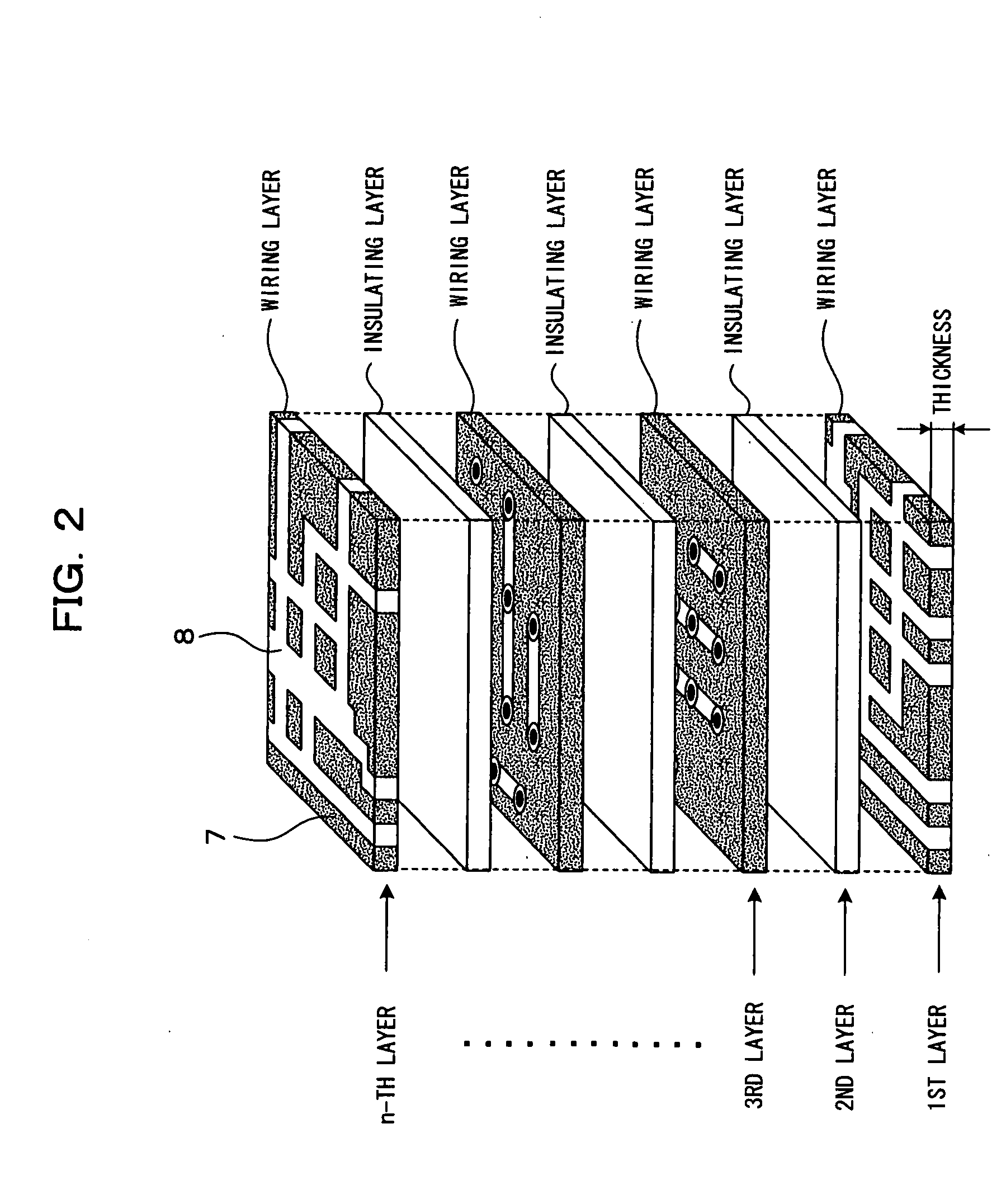
[0096]In the element material determination process as shown in FIG. 3(c) in accordance with the above-mentioned embodiment, physical material property values indicating that “the whole portion is the base material 7” and “the whole portion is the copper foil pattern 8” are determined and processed according to a ratio between the base material 7 and the copper foil pattern 8 for one cell in which the base material 7 and the copper foil pattern 8 are mixed. In this embodiment (Embodiment 2), physical material property values are individually determined according to wiring width of the copper foil pattern 8 of each cell, which is different from the above-mentioned embodiment.

[0097]FIG. 12 and FIG. 13 show Embodiment 2.

[0098]FIG. 12 shows a processing routine in which a material of each cell A in the plane of a single layer model as shown in FIG. 13(a) is determined in an automatic process.

[0099]In steps S1˜S11 of FIG. 12, each cell A is scanned in an x-axis direction as shown in FIG....

embodiment 3

[0122]There have been described the embodiments in which a shape and size of a cell of element division are identical in planes of all single layer models. Alternatively, a model scale can be reduced by setting a shape and size of a cell of element division different from other ranges in the plane of a single layer model in which in-plane deformation does not occur or is in a small range.

[0123]That is, an area where the base material 7 and the copper foil pattern 8 are mixed is divided in a smaller size of the cell A as compared with an area occupied by only a material of either the base material 7 or the copper foil pattern 8.

[0124]Specifically, assuming that the remaining copper ratio is read from the data 2 of wiring patterns of the respective layers of the first file M1 with respect to cells roughly divided in advance and the remaining copper ratio of less than or equal to 20% is occupied by the base material 7, the roughly divided cells are not more finely divided. Since it is ...


PUM


Abstract

A method for analyzing a component mounting board comprising a step (A) for forming a multilayer substrate shell model of a multilayer wiring board, a step (B) for forming a multilayer component shell model divided by element division lines based on the bonding position of a component to the surface of the multilayer wiring board, step (C) for redividing the mounting position of the component in the multilayer substrate shell model, and step (D) for forming an analysis model by bonding the neutral plane of the substrate and the neutral plane of the component through one of a beam element and a solid element, i.e. a bonding element equivalent to mounting conditions of the component, wherein precision of analysis is enhanced while reducing computation cost by performing calculation while imparting boundary conditions to the analysis model.

Description

[0001]The present application is based on International Application No. PCT / JP2006 / 300834, filed Jan. 20, 2006 which application claims priority to Japanese Patent Applications Nos. 2005-066935, filed Mar. 10, 2005, 2005-202372, filed Jul. 12, 2005 and 2005-269312, filed Sep. 16, 2005, the entire contents of which are hereby incorporated by reference.TECHNICAL FIELD[0002]The present invention relates to a method for analyzing physical properties of a component mounting board in a state in which components are mounted to a multilayer wiring board used to construct electric circuits of various electronic devices.BACKGROUND ART[0003]For the purpose of miniaturizing an electronic device, a multilayer wiring board has recently been adopted to construct an electronic circuit for high density mounting of an electronic component. In terms of a wiring pattern of each layer of the multilayer wiring board, a multilayer wiring pattern satisfying electric performance may be obtained by inputting...

Claims


Application Information

Patent Timeline
Patent Type & Authority Applications(United States)
IPC IPC(8): G06F17/50H05K3/32
CPCG06F17/5018G06F2217/40H05K3/0005H05K1/181G06F2217/80G06F30/23G06F2113/18G06F2119/08
Inventor KAKINO, MANABUOKAZAKI, TORUIWASE, TEPPEITAKADA, KAZUNORIFUJIWARA, HIROAKIKUROISHI, TOMOAKI
Owner GK BRIDGE 1
Why Eureka
Try Eureka