Substrate surface temperature measurement method, substrate processing apparatus using the same, and semiconductor device manufacturing method

a substrate processing apparatus and surface temperature technology, applied in semiconductor/solid-state device testing/measurement, heat measurement, instruments, etc., can solve the problems of increasing the cost of the substrate processing apparatus itself, affecting and unable to accurately obtain the thickness of the film during formation and the composition of the film. to achieve the effect of improving the measurement accuracy of the substrate surface temperatur

Inactive Publication Date: 2009-09-03
CANON ANELVA CORP
View PDF12 Cites 19 Cited by
  • Summary
  • Abstract
  • Description
  • Claims
  • Application Information

AI Technical Summary

Benefits of technology

[0027]It is an object of the present invention to provide a surface temperature measurement method that can solve one of the problems described above, and a substrate processing apparatus which utilizes this method. It is another object of the present invention to improve the measurement accuracy of the substrate surface temperature.

Problems solved by technology

An error may occur in measurement when an observation window to observe the substrate is contaminated with a film forming gas.
Also, as the radiation thermometer itself is expensive, it increases the cost of the substrate processing apparatus itself.
It is, however, very difficult to accurately obtain the thickness of the film during formation and the composition of the film.
Therefore, it is difficult to set the calibration parameter correctly.
In this manner, although measurement using the radiation thermometer is advantageous in that it allows noncontact observation, the accuracy may be degraded by various measurement errors, and the radiation thermometer itself is expensive.
If, however, a temperature distribution exists in the substrate, the temperature difference between the average temperature and surface temperature of the substrate increases, thus increasing the error.
This causes an error in temperature measurement.
It is thus difficult to accurately measure the surface temperature of the substrate only from the expansion amount of the substrate.
When bringing the sensor into contact with the substrate surface in this manner, or when the substrate expands by a temperature change in the substrate, it is difficult to maintain the contact state of the sensor with the substrate.
Also, as the thermocouple itself is heated by the heater, an error may occur.
Since the film is not formed on that portion of the substrate which is in contact with the sensor, the substrate is partly wasted.

Method used


Image

  • Substrate surface temperature measurement method, substrate processing apparatus using the same, and semiconductor device manufacturing method
  • Substrate surface temperature measurement method, substrate processing apparatus using the same, and semiconductor device manufacturing method
  • Substrate surface temperature measurement method, substrate processing apparatus using the same, and semiconductor device manufacturing method

Examples


first embodiment

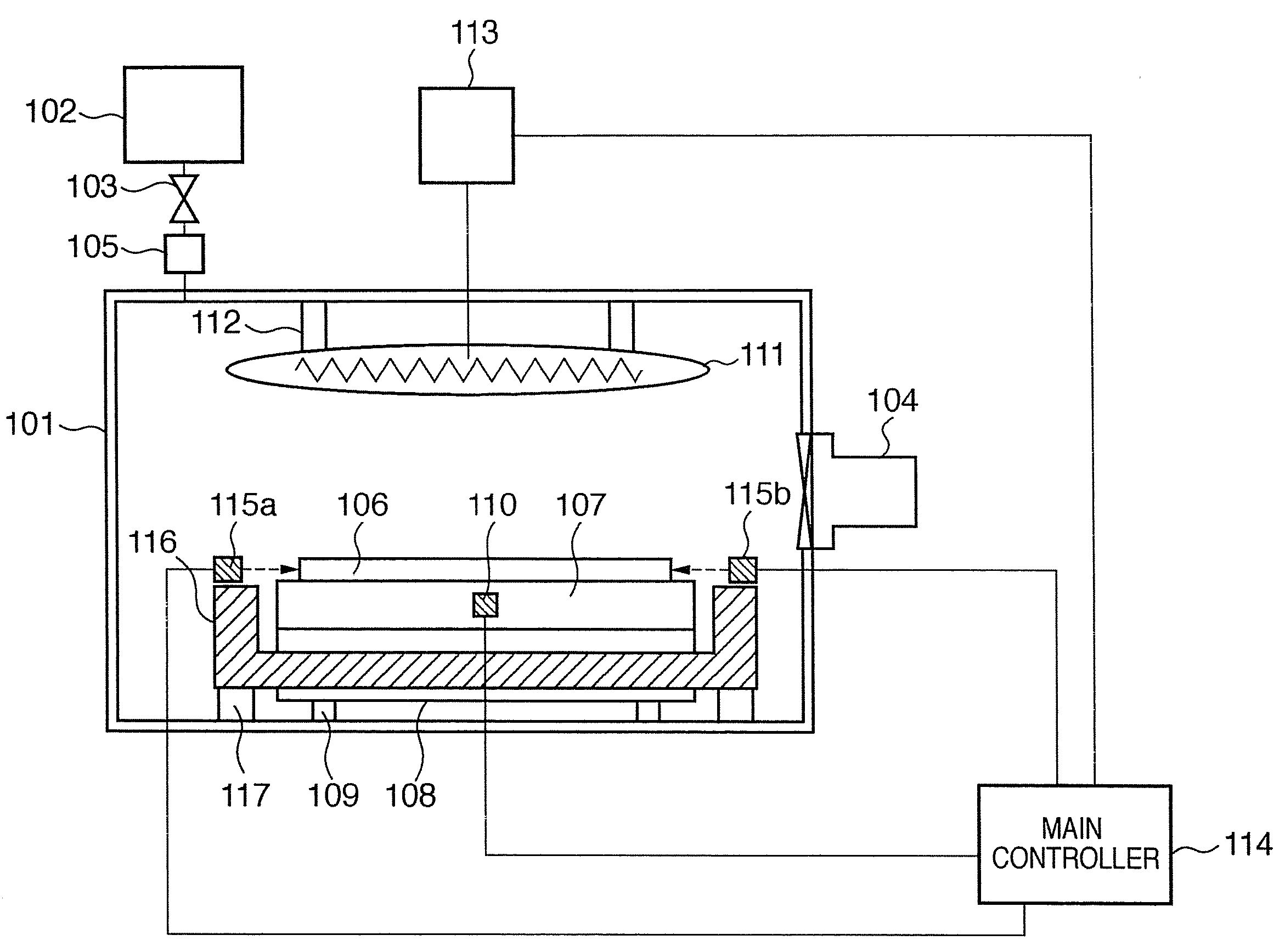
[0069]FIG. 1 schematically shows the arrangement of a thermal CVD apparatus according to the first embodiment of the present invention.

[0070]A substrate processing apparatus employed as the thermal CVD apparatus of this embodiment includes a vacuum vessel 101 and forms a film on a substrate 106 in the vacuum vessel 101. A source gas supply device 102 and vacuum pump 104 are provided to the vacuum vessel 101. The source gas supply device 102 supplies a gas as the source of the film to the vacuum vessel 101. A supply path for the source gas is provided with a valve 103 and a flow controller 105 which adjusts the concentration of the source gas.

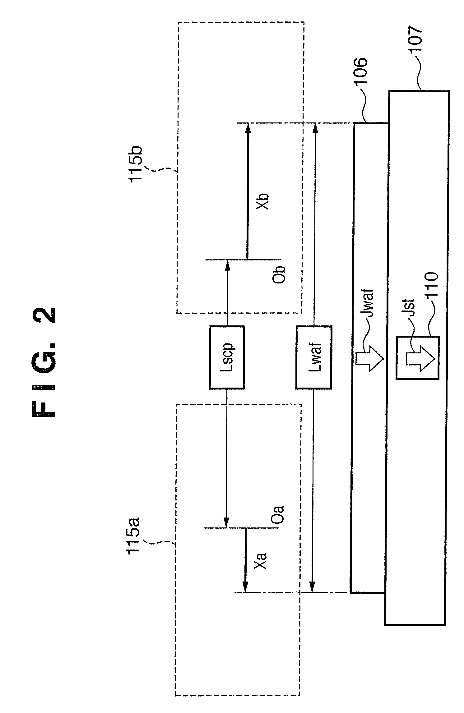
[0071]The vacuum vessel 101 is provided with an electrostatic chuck 107 and substrate stage 108 at its inner bottom. The electrostatic chuck 107 fixes the substrate 106 at a predetermined position. The substrate stage 108 suppresses deformation of the electrostatic chuck 107. The substrate stage 108 is connected to the vacuum vessel 101 through ...

second embodiment

[0101]FIG. 5 schematically shows the arrangement of a thermal CVD apparatus according to the second embodiment of the present invention.

[0102]The apparatus of this embodiment is obtained by adding a scope stage temperature sensor 118 to the arrangement of FIG. 1. The scope stage temperature sensor 118 serves as a support body temperature detection means for detecting the temperature of a scope stage 116. In addition, a scope stage temperature controlling pipe 119 and scope stage temperature controller 120 are added. The scope stage temperature controlling pipe 119 is laid in the scope stage 116 to adjust the temperature of the scope stage 116. The scope stage temperature controller 120 controls the circulation of a refrigerant flowing in the pipe 119.

[0103]As the refrigerant circulates in the scope stage temperature controlling pipe 119, the temperature nonuniformities in the scope stage 116 can be decreased more than in a scope stage not provided with a scope stage temperature cont...

third embodiment

[0113]FIG. 6 schematically shows the arrangement of a thermal CVD apparatus according to the third embodiment of the present invention. In the description of this embodiment, the same constituent components as those of the apparatuses shown in FIGS. 1 and 5 are denoted by the same reference numerals, and a repetitive description will be omitted.

[0114]In the third embodiment, no halogen heater (see reference numeral 111 in FIGS. 1 and 2) is provided above the substrate surface. As shown in FIG. 6, a heater 121 arranged in a substrate stage 108 heats a substrate 106. The heater 121 is connected to a heater controller 122. The heater controller 122 is connected to a main controller 114.

[0115]The upper surface of the substrate 106 has alignment marks 126 at a plurality of portions. The positions of the alignment marks 126 can be detected by alignment scopes 123a and 123b above them. The alignment scopes 123a and 123b are attached to a scope stage 124. The scope stage 124 is connected to...


PUM

PropertyMeasurementUnit
thicknessaaaaaaaaaa
surface temperatureaaaaaaaaaa
temperatureaaaaaaaaaa

Abstract

The expansion amount of a substrate (106) is measured using a scope (115a, 115b) which observes the edge surface of the substrate (106). The temperature of the neutral plane of the substrate (106) is calculated using the expansion amount of the substrate (106). A heat flux in the substrate (106) is measured using a heat flux sensor (110). The temperature difference between the neutral surface and upper surface of the substrate (106) is calculated from the measured heat flux and the heat resistance of the substrate (106). The temperature of the surface of the substrate (106) is obtained using the temperature difference and the temperature of the neutral plane of the substrate.

Description

BACKGROUND OF THE INVENTION[0001]1. Field of the Invention[0002]The present invention relates, in an apparatus that heats and cools a substrate in a process of manufacturing an electronic device such as a semiconductor integrated circuit and a display device electron source, to a substrate surface temperature measurement method which measures the substrate surface temperature in-situ, a substrate processing apparatus which uses this method, and a semiconductor device manufacturing method.[0003]2. Description of the Related Art[0004]A semiconductor integrated circuit manufacturing process includes various types of annealing processes such as baking in photolithography, film formation, and ashing. In such an annealing process, conventionally, a target substrate is heated using a halogen lamp arranged to oppose the target substrate, or a heater incorporated in a support body that supports the target substrate.[0005]In this case, a radiation thermometer is arranged on a side opposite to...

Claims


Application Information

Patent Timeline
Patent Type & Authority Applications(United States)
IPC IPC(8): G01K17/00H01L21/66
CPCG01K5/486H01L22/12G01K7/42G01K5/50
Inventor YAMAMOTO, TAKESHI
Owner CANON ANELVA CORP
Why Eureka
Try Eureka