Method and system for detection of wafer centering in a track lithography tool

a lithography tool and track technology, applied in the field of substrate processing equipment, can solve problems such as unwanted contact between optical elements and processing fluids, and achieve the effect of small form factor

Inactive Publication Date: 2008-07-17
SOKUDO CO LTD
View PDF15 Cites 26 Cited by
  • Summary
  • Abstract
  • Description
  • Claims
  • Application Information

AI Technical Summary

Benefits of technology

[0012]Many benefits are achieved by way of the present invention over conventional techniques. For example, embodiments of the present invention provide systems to measure wafer centering that are resistant to contamination from photolithography chemicals. Moreover, embodiments are characterized by a smaller form factor than conventional systems since the

Problems solved by technology

However, in some track lithography tool applications, such wafer centering designs are not practical due to the use of

Method used


Image

  • Method and system for detection of wafer centering in a track lithography tool
  • Method and system for detection of wafer centering in a track lithography tool
  • Method and system for detection of wafer centering in a track lithography tool

Examples


Embodiment Construction

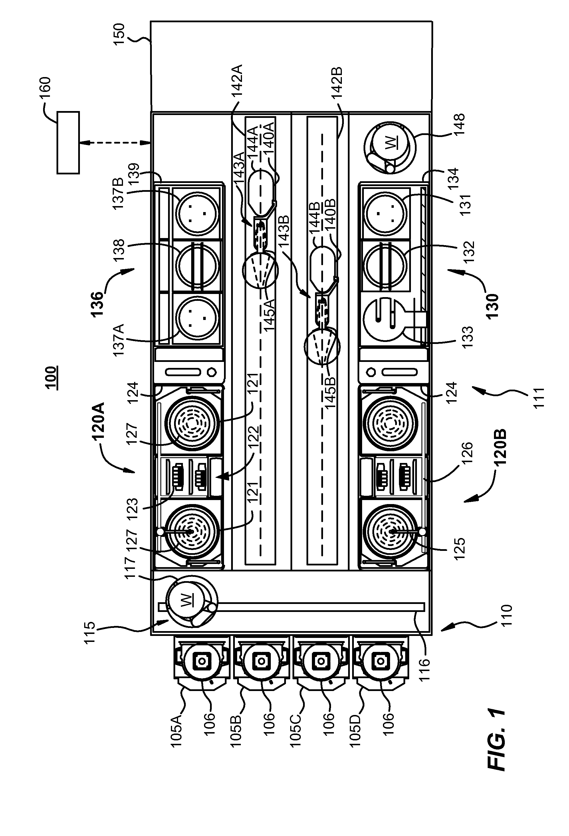
[0022]FIG. 1 is a plan view of an embodiment of a track lithography tool in which the embodiments of the present invention may be used. As illustrated in FIG. 1, the track lithography tool contains a front end module 110 (sometimes referred to as a factory interface) and a process module 111. In other embodiments, the track lithography tool includes a rear module (not shown), which is sometimes referred to as a scanner interface. Front end module 110 generally contains one or more pod assemblies or FOUPS (e.g., items 105A-D) and a front end robot assembly 115 including a horizontal motion assembly 116 and a front end robot 117. The front end module 110 may also include front end processing racks (not shown). The one or more pod assemblies 105A-D are generally adapted to accept one or more cassettes 106 that may contain one or more substrates or wafers that are to be processed in the track lithography tool. The front end module 110 may also contain one or more passthrough positions (...


PUM


Abstract

A system for measuring substrate concentricity includes a substrate support member adapted to rotate a substrate around a substantially vertical axis. The substrate includes a mounting surface and a process surface. The system also includes a spin cup positioned below the substrate and a translatable arm mounted a predetermined distance above the process surface of the substrate. The translatable arm is adapted to translate along a radius of the substrate. The system further includes an optical emitter mounted on the translatable arm and an optical detector mounted on the translatable arm.

Description

CROSS-REFERENCES TO RELATED APPLICATIONS[0001]The present application claims benefit under 35 U.S.C. § 119(e) of U.S. Provisional Patent Application No. 60 / 884,587, filed Jan. 11, 2007, entitled “Method and System for Detection of Wafer Centering in a Track Lithography Tool,” which is incorporated herein by reference in its entirety.BACKGROUND OF THE INVENTION[0002]The present invention relates generally to the field of substrate processing equipment. More particularly, the present invention relates to a method and apparatus for detecting wafer centering during operation of a semiconductor processing apparatus. Merely by way of example, the method and apparatus of the present invention have been applied to the use of an optical emitter and emitter mounted on a translatable stage to determine wafer position during wafer rotation in a process chamber of a track lithography tool. The method and apparatus can be applied to other processing devices for semiconductor processing equipment ...

Claims


Application Information

Patent Timeline
IPC IPC(8): G01D21/00
CPCG01D5/342
Inventor HERCHEN, HARALDPANG, LILYPORRAS, ERICA
Owner SOKUDO CO LTD
Why Eureka
Try Eureka