Method and Apparatus For Fabricating Polycrystalline Silicon Film Using Transparent Substrate

a technology of polycrystalline silicon and transparent substrate, which is applied in the direction of coatings, solid-state devices, chemical vapor deposition coatings, etc., can solve the problems of high cost of materials, high temperature process risk, and the formation of polycrystalline silicon electronic devices using silicon or quartz substrates

Inactive Publication Date: 2008-07-17
POINT ENG
View PDF14 Cites 6 Cited by
  • Summary
  • Abstract
  • Description
  • Claims
  • Application Information

AI Technical Summary

Benefits of technology

[0012]In a yet another aspect of the present invention, there is provided a method for fabricating a Field Effect Transistor (FET) having a transparent substrate, a polycrystalline silicon active layer formed on the transparent substrate, a gate insulating layer formed on the polycrystalline silicon active layer, and a gate formed on the gate insulating layer. The forming of the polycrystalline silicon active layer further includes forming a light absorption layer on a surface of the transparent substrate; and heating the light absorption layer using irradiation of an RTP light source, while depositing a polycrystalline silicon film on the light absorption layer.

Problems solved by technology

In general, a polycrystalline silicon electronic device formed using a silicon or quartz substrate has a disadvantage that material is expensive.
However, the transparent substrate has a critical disadvantage that it is vulnerable to a high temperature process (600° C. or more).
Accordingly, a thermal damage or deformation of the substrate is frequently caused.
Therefore, the amorphous silicon poly-crystallization method has a drawback that a yield is low and a crystallization time is long taken.
The vapor deposition method cannot use the transparent substrate of the cheap glass or plastic having a low softening temperature, because the polycrystalline silicon film should be deposited at a high temperature of 600° C. or more.
Therefore, the vapor deposition method is disadvantageous in cost aspect.

Method used


Image

  • Method and Apparatus For Fabricating Polycrystalline Silicon Film Using Transparent Substrate
  • Method and Apparatus For Fabricating Polycrystalline Silicon Film Using Transparent Substrate
  • Method and Apparatus For Fabricating Polycrystalline Silicon Film Using Transparent Substrate

Examples


Embodiment Construction

[0025]Reference will now be made in detail to the preferred embodiments of the present invention, examples of which are illustrated in the accompanying drawings. Wherever possible, the same reference numerals will be used throughout the drawings to refer to the same or like parts.

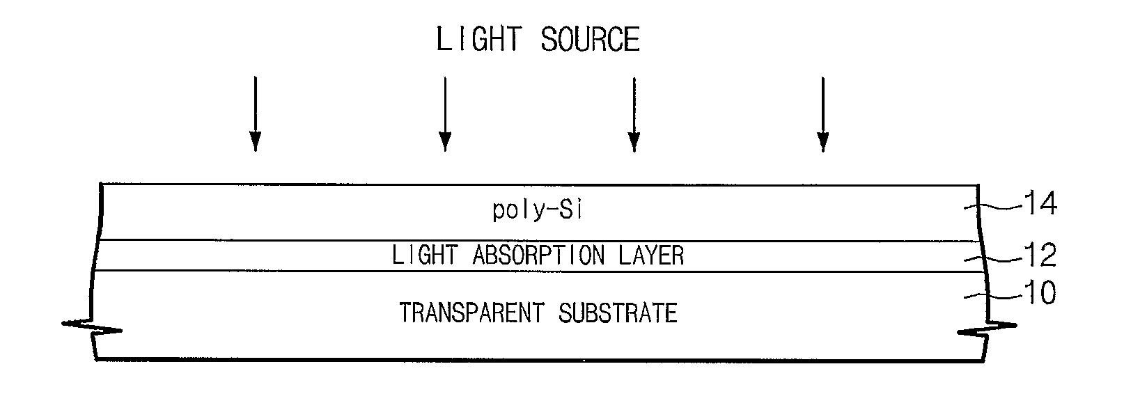
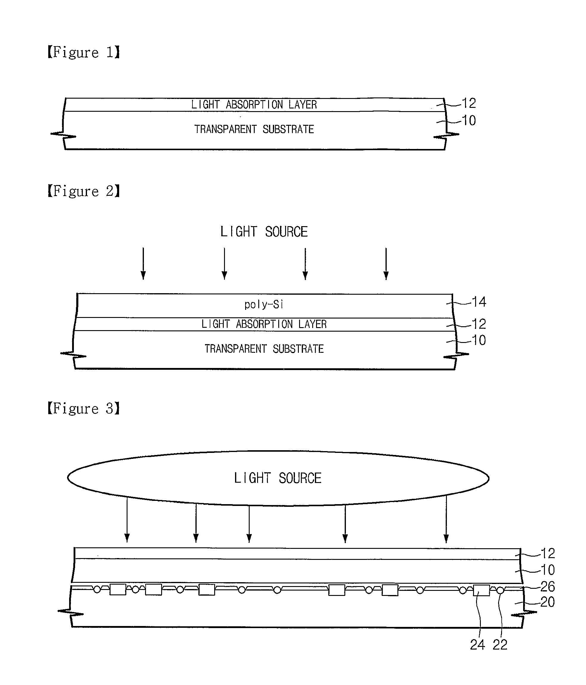
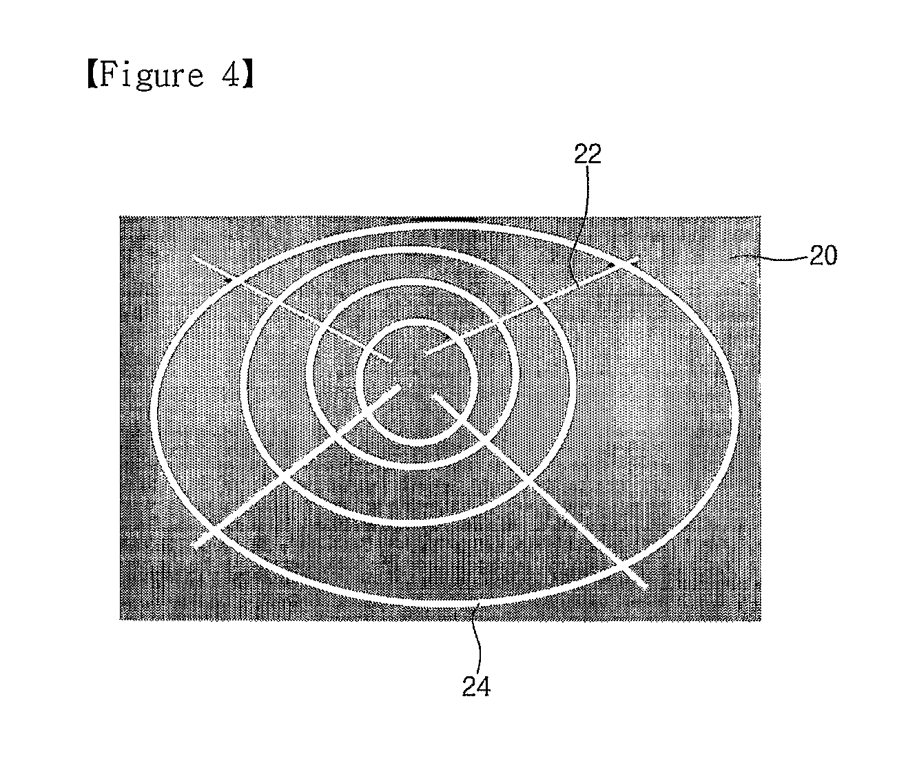
[0026]FIGS. 1 and 2 are process diagrams illustrating a method for fabricating a polycrystalline silicon film using a transparent substrate according to the present invention. FIG. 3 is a diagram illustrating a state in which the transparent substrate is safely mounted on a substrate holder in the method for fabricating the polycrystalline silicon film using the transparent substrate according to the present invention. FIG. 4 is a plan view illustrating the substrate holder according to the present invention.

[0027]As shown in FIG. 1, a light absorption layer 12 is deposited on the transparent substrate 10 at about 500° C. or less using a low temperature Plasma Enhanced Chemical Vapor Deposition (PECVD) and ...


PUM

PropertyMeasurementUnit
temperatureaaaaaaaaaa
pressureaaaaaaaaaa
deformation temperatureaaaaaaaaaa

Abstract

Provided is a method and apparatus for fabricating a polycrystalline silicon film using a transparent substrate. The method includes forming a light absorption layer on a surface of the transparent substrate; and heating the light absorption layer using irradiation of Rapid Thermal Process (RTP) light source, while depositing the polycrystalline silicon film on the light absorption layer.

Description

TECHNICAL FIELD[0001]The present invention relates to a method and apparatus for fabricating a polycrystalline silicon film, and a structure thereof, and more particularly, to a method and apparatus for fabricating a polycrystalline silicon film using a transparent substrate, for providing an excellent electrical characteristic by using a Rapid Thermal Process (RTP) light source as, not a heat treatment source, an energy source for depositing polycrystalline silicon by an RTP and a Chemical Vapor Deposition (CVD).BACKGROUND ART[0002]Polycrystalline silicon (Poly-Si) is being applied to various electronic devices, e.g. a Thin Film Transistor (TFT) device as well as a solar cell because it has an excellent electrical characteristic compared with amorphous silicon (a-Si). In general, a polycrystalline silicon electronic device formed using a silicon or quartz substrate has a disadvantage that material is expensive. In consideration of the disadvantage, a transparent substrate of cheap ...

Claims


Application Information

Patent Timeline
Patent Type & Authority Applications(United States)
IPC IPC(8): H01L29/04H01L21/205H01L21/336C23C16/00
CPCH01L27/1214H01L29/78675H01L29/78603H01L27/1259
Inventor AHN, BUM MO
Owner POINT ENG
Why Eureka
Try Eureka