Method And Apparatus For A Semiconductor Structure

a semiconductor structure and method technology, applied in the field of one or more solar modules, can solve the problems of reducing the efficiency of solar cells, so as to reduce waste of light adsorption, and reduce the negative effect of surface defects

Inactive Publication Date: 2008-07-24
GENERAL ELECTRIC CO
View PDF22 Cites 108 Cited by
  • Summary
  • Abstract
  • Description
  • Claims
  • Application Information

AI Technical Summary

Benefits of technology

[0035]Generally, the embodiments discussed herein can provide passivation techniques to minimize the negative effects of surface defects, and have a smaller absorption coefficient to minimize wasteful light adsorption in the front of the structure. Particularly, the absorption coefficient of crystalline silicon is generally much smaller than amorphous silicon. Thus, utilizing a crystalline silicon layer can allow more light to be absorbed in the region where it contributes to the cell performance, rather than in the front of the structure. The present invention can also provide a field effect for minimizing the recombination of charge carriers. Particularly, n+ or p+ di

Problems solved by technology

Moreover, poly-crystalline semiconductor materials may contain randomly-oriented grains, with grain boundaries which induce a large number of bulk and surface defect sites.
The presence of various defects of this type can be the source of deleterious effects in the photovoltaic device.
Thus, they become lost as current carriers.
Generally, an amorphous layer on the front of a photovoltaic device can result in absorption of light, which is thus lost from the cell.
Any light absorbed in the passivation layer can contribute to a leakage current and can be lost.
The mechanism for this loss is that charge carriers generated in the amorphous intrinsic layer may cause recombination at the interface with charge carriers generated in the crystalline sil

Method used


Image

  • Method And Apparatus For A Semiconductor Structure
  • Method And Apparatus For A Semiconductor Structure
  • Method And Apparatus For A Semiconductor Structure

Examples


Embodiment Construction

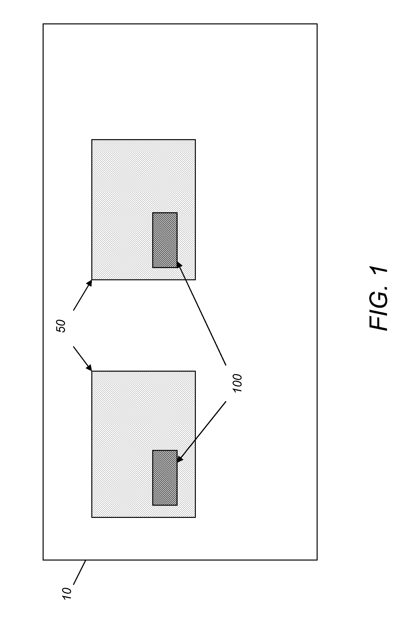
[0045]As depicted in FIG. 1, one exemplary embodiment of a solar module 10 can include a plurality of solar cell devices 50. Particularly, each solar cell device 50 may further include at least one or more semiconductor structures 100.

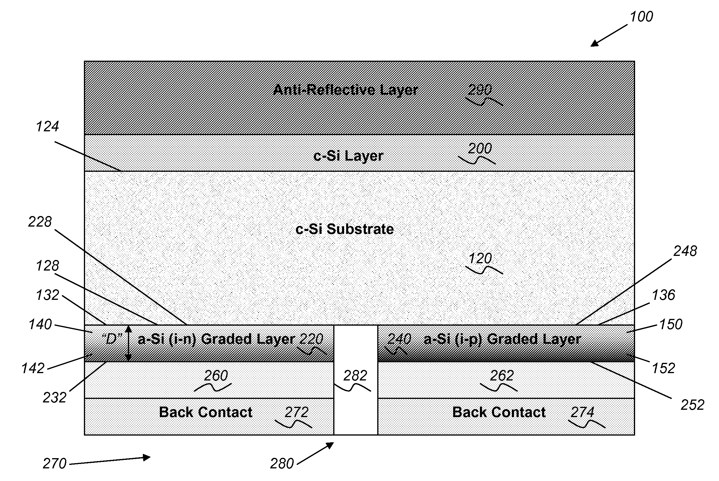
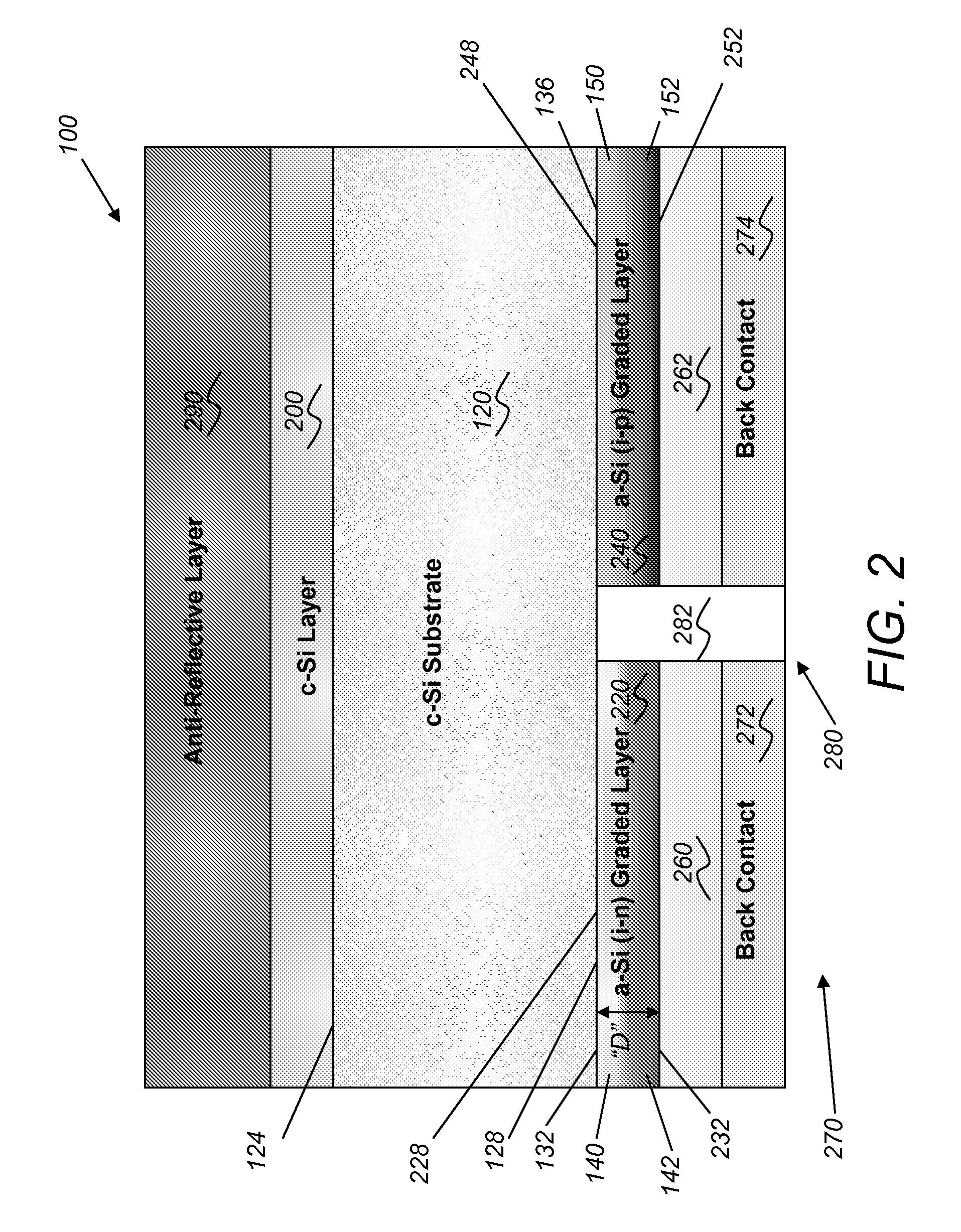
[0046]As depicted in FIG. 2, an exemplary semiconductor structure 100 can include a substrate 120, a first semiconductor layer 200, a second semiconductor layer 220, a third semiconductor layer 240, a first electrode layer 260, a second electrode layer 262, at least one electrical contact 270, and a transparent or anti-reflective layer 290. Generally, the substrate 120 can include a front surface 124 and a back surface 128. The substrate 120 usually has a thickness of about 50 microns-about 600 microns. The substrate 120 can be a crystalline silicon, such as a multi-crystalline, including one or more dopants, such as a p-type or an n-type, or a mono-crystalline silicon. Desirably, the substrate 120 is an n-type-mono-crystalline silicon. A multi-crystal...


PUM


Abstract

One exemplary embodiment is a semiconductor structure, that can include a semiconductor substrate of one conductivity type, having a front surface and a back surface, a first semiconductor layer disposed on the front surface of the semiconductor substrate, a second semiconductor layer disposed on a portion of the back surface of the semiconductor substrate, and a third semiconductor layer disposed on another portion of the back surface of the semiconductor substrate. Each of the second and third semiconductor layers may be compositionally graded through its depth, from substantially intrinsic at an interface with the substrate, to substantially conductive at an opposite side, and have a selected conductivity type obtained by the incorporation of one or more selected dopants.

Description

CROSS-REFERENCE TO RELATED APPLICATIONS[0001]Non-provisional application no. ______, entitled, “METHOD AND APPARATUS FOR A SEMICONDUCTOR STRUCTURE FORMING AT LEAST ONE VIA”, filed, by Korevaar et al. (Attorney Docket No. 218410-1) and application Ser. No. 11 / 480,161, entitled, “PHOTOVOLTAIC DEVICE WHICH INCLUDES ALL-BACK-CONTACT CONFIGURATION; AND RELATED PROCESSES”, filed Jun. 30, 2006, for Johnson et al. are incorporated by reference in their entirety.FIELD[0002]The embodiments described herein generally relate to one or more solar modules. More specifically, the embodiments relate to one or more solar modules based on at least one semiconductor structure.BACKGROUND[0003]There is no doubt that solar energy offers the potential for providing virtually unlimited energy for man, if the solar energy can be made available in a useful form. Perhaps the greatest effort so far has been using the sun's energy to obtain electricity, which can then be utilized through any existing electrical...

Claims


Application Information

Patent Timeline
IPC IPC(8): H01L31/036H01L31/18
CPCH01L31/0236H01L31/036H01L31/03687H01L31/065Y02E10/50H01L31/077H01L31/1816H01L31/1868H01L31/204H01L31/0747Y02E10/547Y02P70/50
Inventor KOREVAAR, BASTIAAN ARIEJOHNSON, JAMES NEIL
Owner GENERAL ELECTRIC CO
Why Eureka
Try Eureka