Method of manufacturing dual gate oxide devices

a technology of oxide devices and gate oxides, which is applied in the manufacturing of semiconductor/solid-state devices, basic electric elements, electric devices, etc., can solve the problems of photoresist residues, process defects, and photoresist effects, and achieve the effects of improving the density of photoresist, reducing the risk of photoresist defects, and improving the resistance to acid solutions

Active Publication Date: 2014-11-20
SHANGHAI HUALI MICROELECTRONICS CORP
View PDF8 Cites 0 Cited by
  • Summary
  • Abstract
  • Description
  • Claims
  • Application Information

AI Technical Summary

Benefits of technology

[0025]The method of manufacturing dual gate oxide devices in the present invention can effectively enhance the density of the photoresist before the etching, process so, as to improve its erosion-resistance to acid solutions and reduce the risk of forming photoresist defects during the etching process. Additionally, the linewidth of the photoresist pattern increases 10 nm to 20 nm by the chemical curing treatment utilizing the RELACS material, which will, compensate the 10 nm to 30 nm linewidth decrease of the photoresist pattern due to the UV radiation, so that the effects on the device linewidth by the manufacturing process can be minimized.

Problems solved by technology

However, when the acid solution etches the silicon oxide thin film 13, it also makes effects on the photoresist 14 and forms process defects mainly including photoresist residue and SiC deposition.
However, there still exist some problems to be solved in the conventional methods of preventing photoresist defects mentioned above.
In the first method, the baking temperature cannot be too high and the baking time cannot be too long, otherwise the photolithography patterns of the photoresist will be deformed, which may further have negative effects on the throughput.
Moreover, the density of the baked photoresist layer may not meet the requirements of erosion-resistance to acid solutions due to the temperature and time limitations.
In the second method, the UV curing process which is performed after the photolithography process may result in contractions in the thickness of the photoresist layer and the linewidth of the photoresist pattern.
As a result, the linewidth as well as the quality of the dual gate oxide device to be formed later may be affected.

Method used


Image

  • Method of manufacturing dual gate oxide devices
  • Method of manufacturing dual gate oxide devices
  • Method of manufacturing dual gate oxide devices

Examples


Embodiment Construction

[0029]The method of manufacturing dual gate oxide devices of the present invention will be described in further details hereinafter with respect to the embodiments and the accompanying drawings.

[0030]The present invention is described with reference to the attached figures, wherein like reference numerals are used throughout the figures to designate similar or equivalent elements. The figures are not drawn to scale and they are provided merely to illustrate the invention. It should be understood that numerous specific details, relationships, and methods are set forth to provide an understanding of the invention. One skilled in the relevant art, however, will readily recognize that the invention can be practiced without one or more of the specific details or with other methods. In other instances, well-known structures or operations are not shown in detail to avoid obscuring the invention.

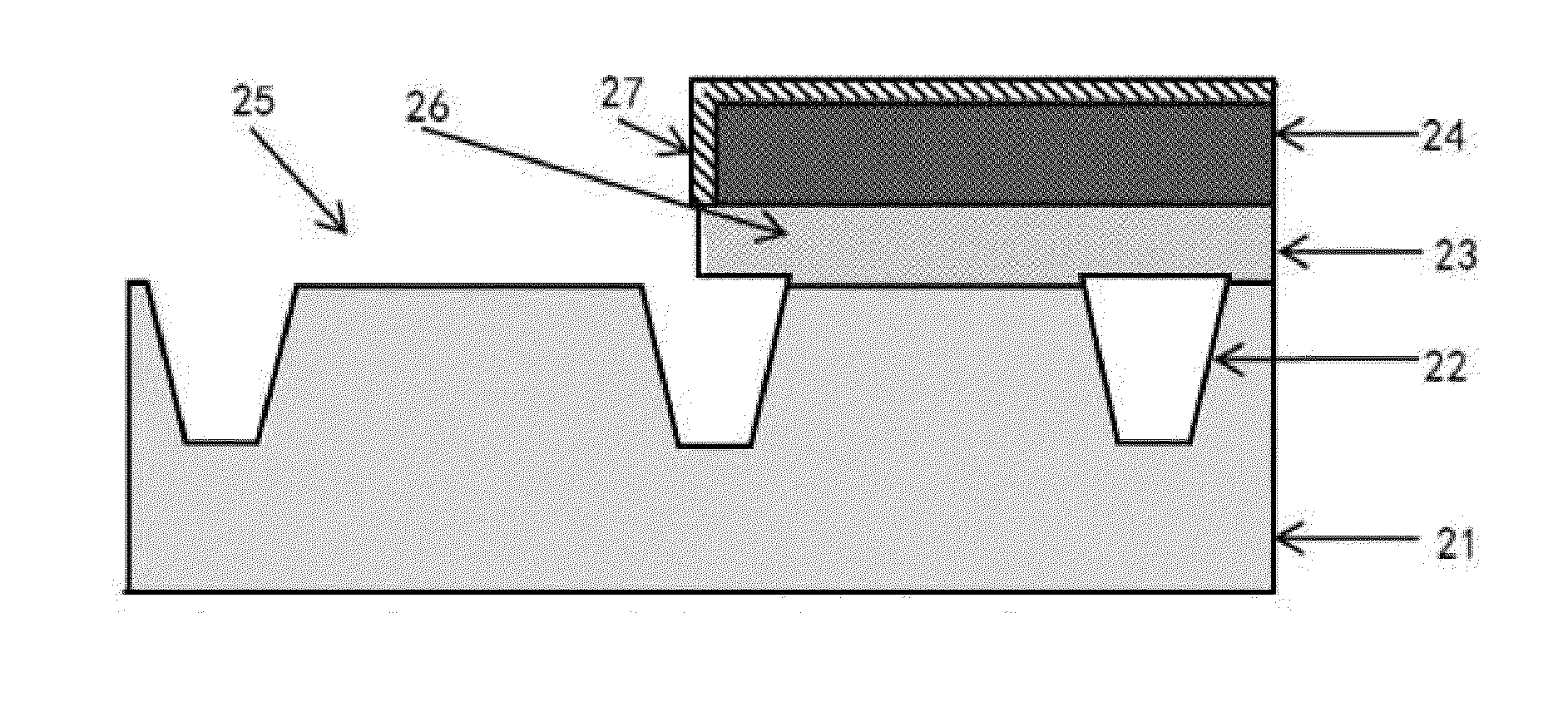
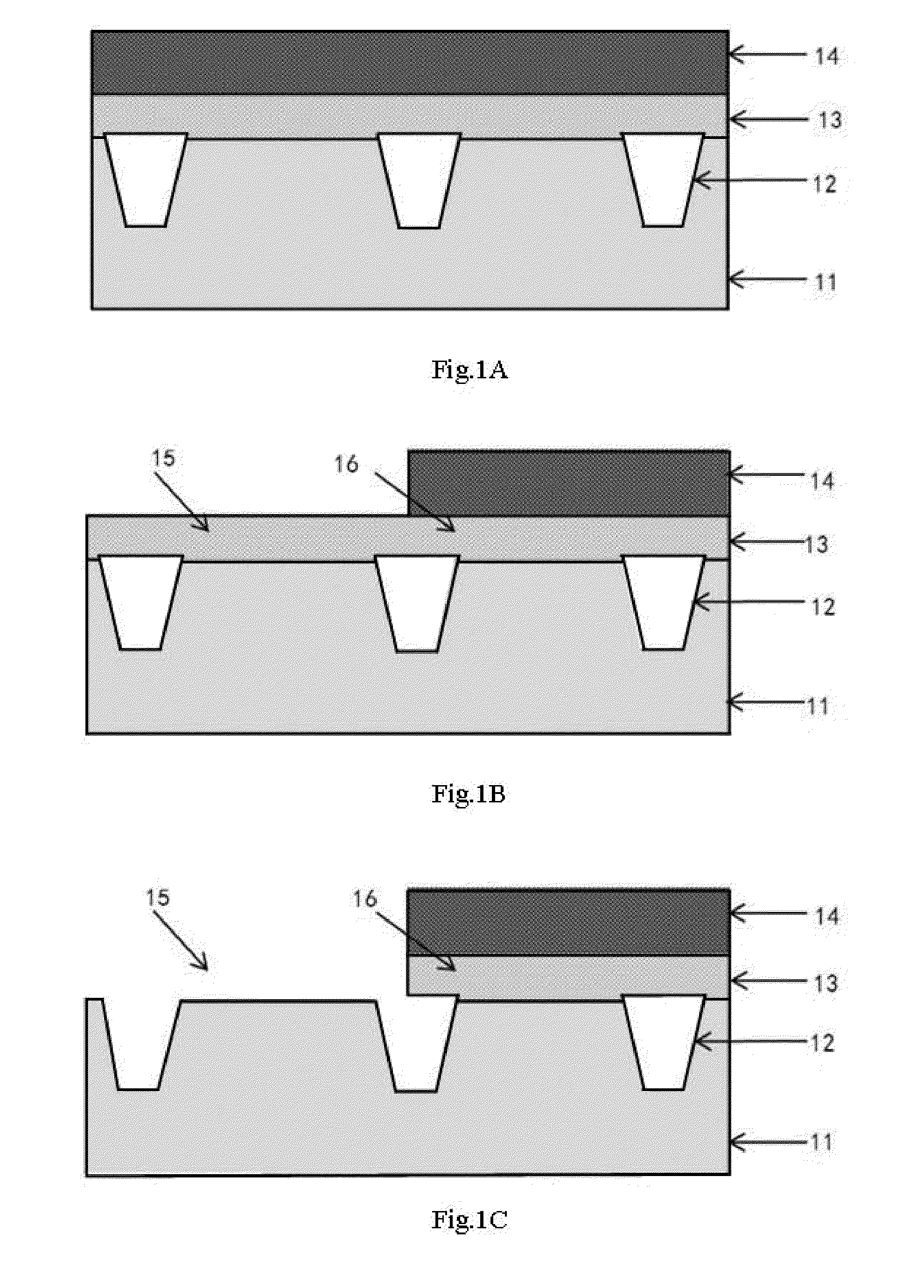
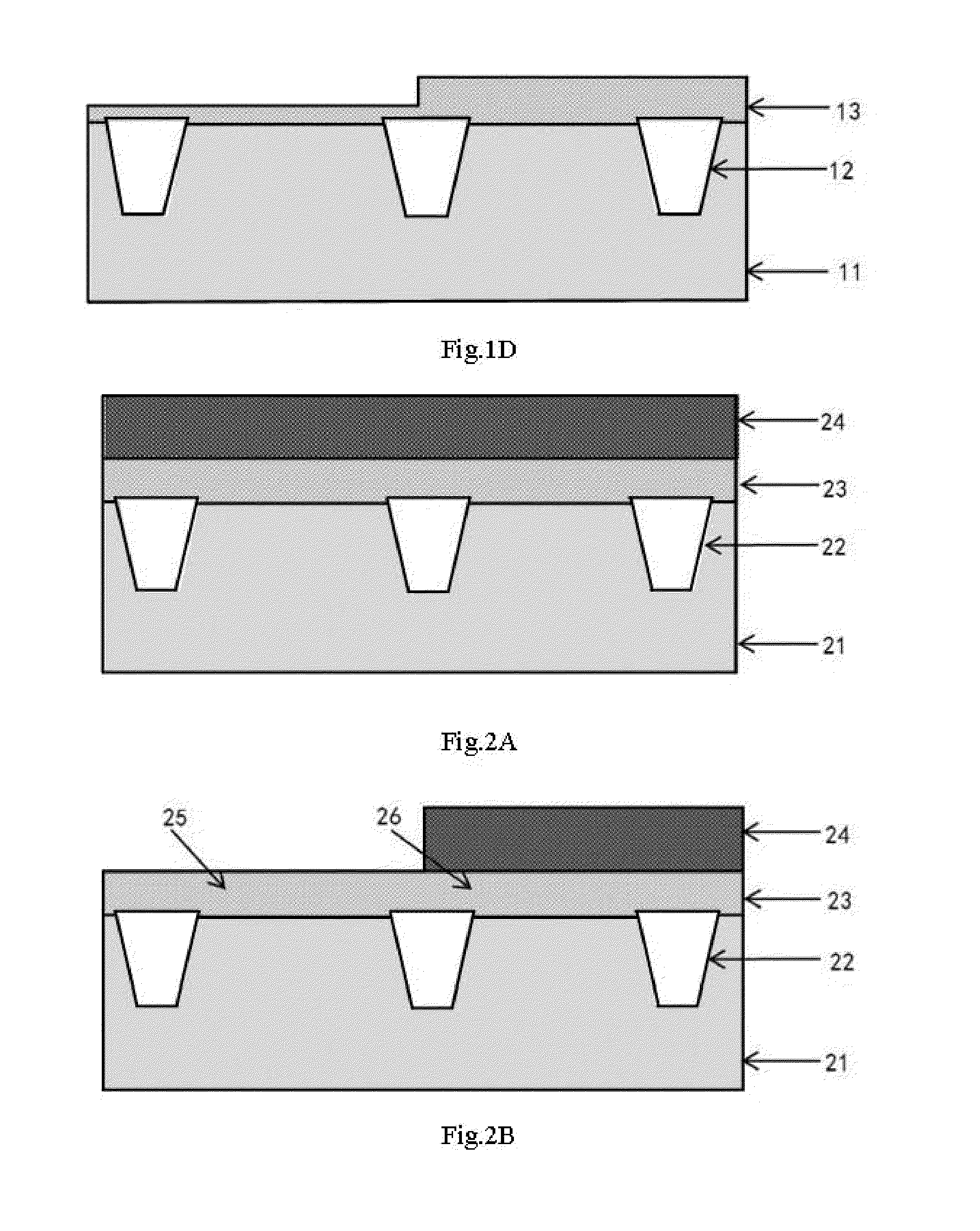
[0031]Referring to FIG. 2A to FIG. 2E, in one embodiment of the present, invention, the method o...


PUM


Abstract

The present invention provides method of manufacturing dual gate oxide devices. The method comprises coating photoresist on the substrate which is deposited by an oxide thin film; removing some of the photoresist by exposure and development to divide the oxide thin film into a first area to be etched and a second area coated by the remained photoresist; coating RELACS material on the remained photoresist and heating to form a protective film based on the crosslinking reaction between the RELACS material and the high molecular compounds in the photoresist; performing UV radiation to strengthen and cure the protective film; removing the oxide thin film in the first area by etching and removing the remained photoresist; and depositing again an oxide film to form an oxide layer of different thickness in the first area and the second area so as to form a dual gate oxide structure.

Description

CROSS-REFERENCE TO RELATED APPLICATION[0001]This application claims the priority benefit of China application serial no. 201310177577.5, filed May 14, 2013. All disclosure of the China application is incorporated herein by reference.FIELD OF THE INVENTION[0002]The present invention relates to the field of semiconductor fabrication technology and particularly to a method of manufacturing dual gate oxide devices.BACKGROUND OF THE INVENTION[0003]With the development of semiconductor technology, one integrated circuit (IC) chip will integrate pluralities of functional devices, which comprise different Field Effect Transistors (FETs) respectively. The multiple gate oxide process has become a common method to form different FETs in a same chip.[0004]Nowadays, varieties of multiple gate oxide processes are provided. FIG. 1A to FIG. 1D show cross-sectional views of a dual gate oxide device in the conventional manufacturing process. As shown in FIG. 1A, the silicon substrate 11 with shallow ...

Claims


Application Information

Patent Timeline
Patent Type & Authority Applications(United States)
IPC IPC(8): H01L21/311
CPCH01L21/31144H01L21/823462H01L21/0273H01L21/0274H01L21/32139H01L21/0337H01L21/3088H01L21/28123H01L21/0338
Inventor HUANG, JUNMAO, ZHIBIAOCHONG, ERMIN
Owner SHANGHAI HUALI MICROELECTRONICS CORP
Why Eureka
Try Eureka