Semiconductor device and method for manufacturing the same
a technology of insulated gate bipolar transistor and semiconductor device, which is applied in the direction of semiconductor device, basic electric element, electrical apparatus, etc., can solve the problems of lowering destruction resistance and large and achieves lowering destruction resistance in short-circuit test, preventing the effect of short-circuit test fluctuation, and suppressing the fluctuation of on voltag
- Summary
- Abstract
- Description
- Claims
- Application Information
AI Technical Summary
Benefits of technology
Problems solved by technology
Method used
Image

Examples
first embodiment
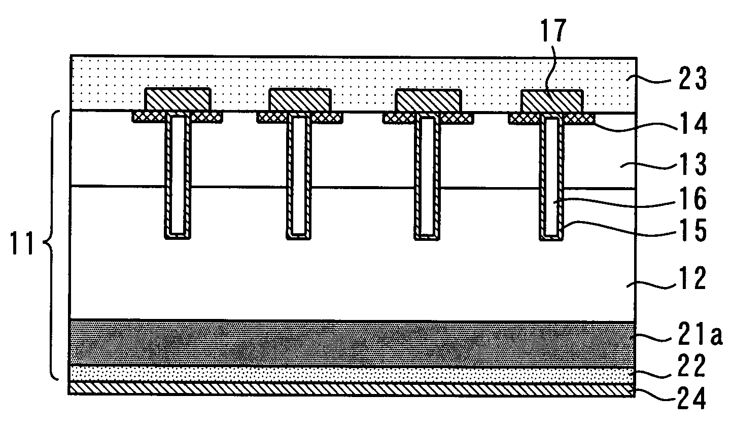
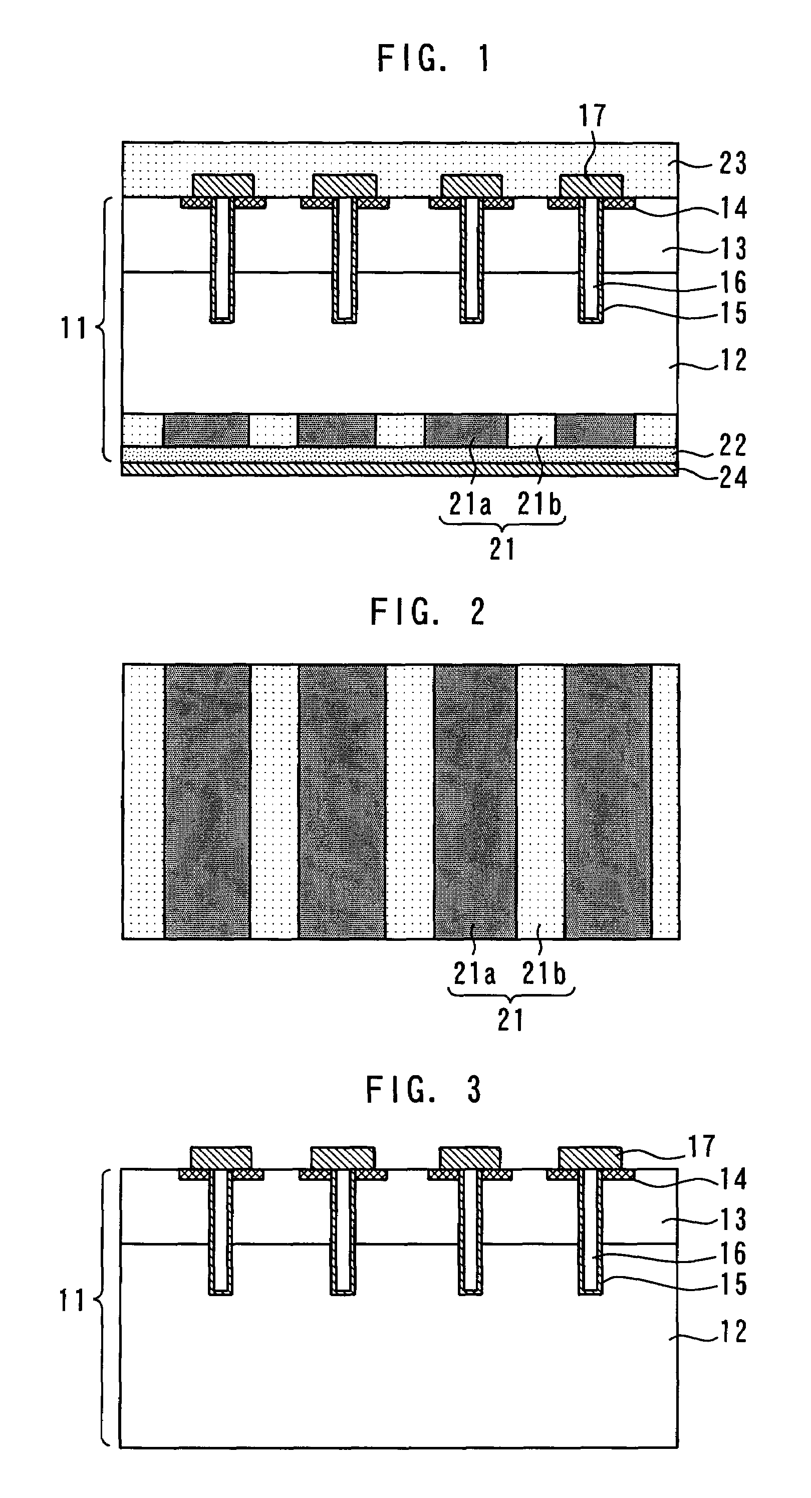
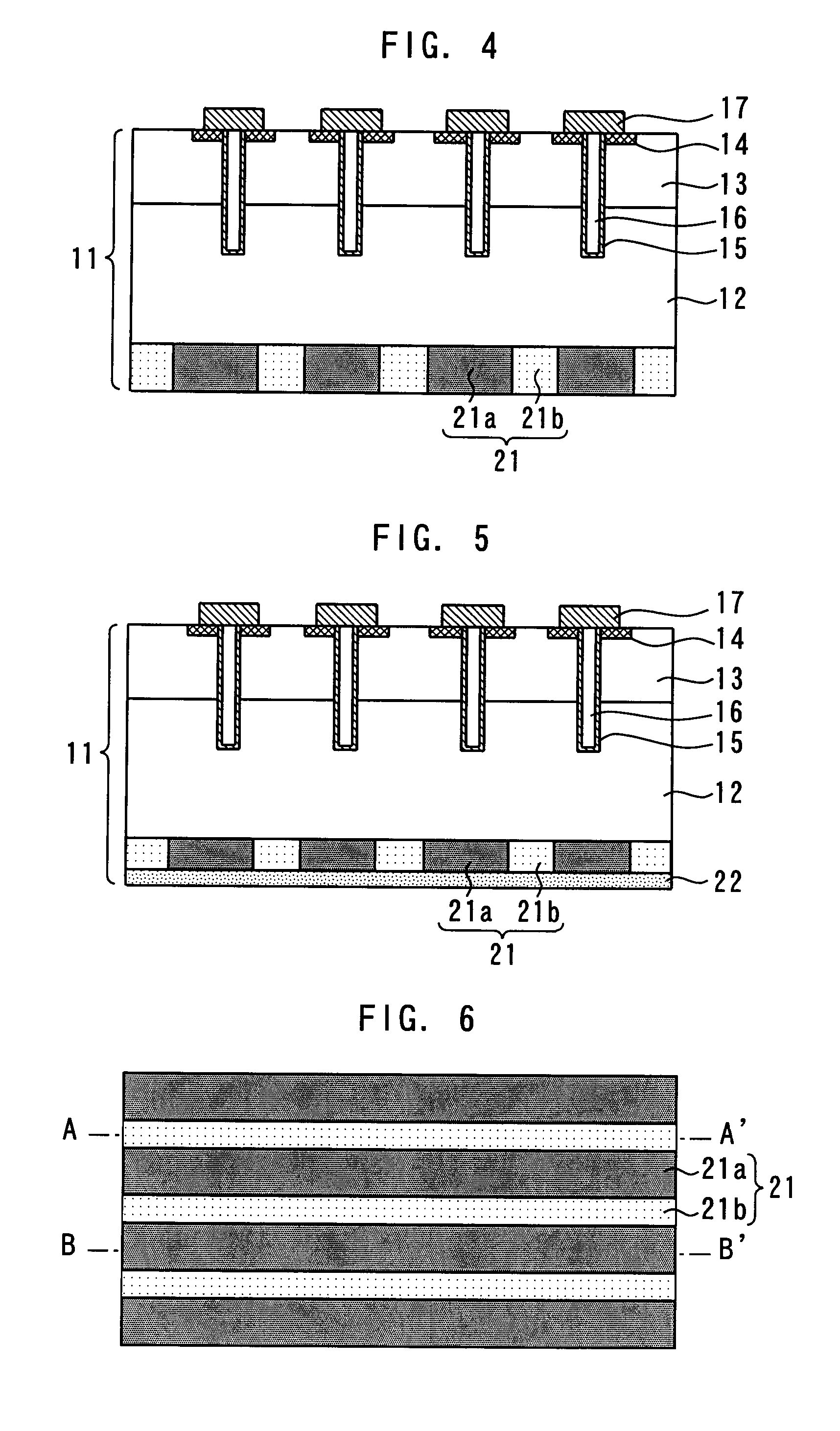
[0027]FIG. 1 is a sectional view showing a semiconductor device according to the first embodiment of the present invention. On the upper surface (first major surface) of a wafer 11, a plurality of MOSFETs, each having an N-channel, are formed in a stripe. Specifically, a P-base layer 13 is formed on an N−-drift layer 12, and an N+-emitter layers 14 are formed on the surface of parts of the P-base layer 13. Trenches are formed so as to penetrate the N+-emitter layers 14, and gate electrodes 16 are formed in the trenches via gate insulating films 15. On the gate electrodes 16, insulating films 17 are formed.
[0028]On the lower surface (second major surface) of the wafer 11, an N-buffer layer 21 is formed. On the lower surface side of the wafer 11, lower than the N-buffer layer 21, a P-collector layer 22 is formed. An emitter electrode 23 is formed on the upper surface of the wafer 11, and a collector electrode 24 is formed on the lower surface of the wafer 11. FIG. 2 is a plan view sho...
second embodiment
[0035]In the first embodiment, the direction of the stripe of the highly activated portions 21a and the lowly activated portions 21b in the N-buffer layer 21 was in parallel to the direction of the stripe of a plurality of MOSFETs. In this case, to realize stable operation by equalizing carrier distribution in the IGBT when the IGBT is turned on, the distance between the highly activated portions 21a and the lowly activated portions 21b must be multiples of the stripe pitch of the plurality of MOSFETs. However, since the beam diameter of laser beams is larger than the stripe pitch of the MOSFET, the irradiation accuracy of the laser beams is tight, and realization is difficult.
[0036]Therefore, in the second embodiment, in the step of forming the N-buffer layer 21, the direction of the stripe of the regions to perform and not perform laser annealing treatment is made perpendicular to the direction of the stripe of the plurality of MOSFETs. Other steps are the same as the steps in the...
third embodiment
[0039]FIG. 9 is a sectional view showing a semiconductor device according to the third embodiment of the present invention. In the circumference of the region for forming a plurality of MOSFETs, guard rings 25 (field limiting rings: FLRs) are formed on the upper surface of the wafer 11. Highly activated portions 21a are formed on the entire surface of the N-buffer layer 21 corresponding to the region for forming the guard rings 25. Other configurations are the same as the configurations of the first embodiment.
[0040]In the manufacturing process of the semiconductor device according to the third embodiment, in addition to the process of the first embodiment, guard rings 25 are formed in the circumference of the region for forming of a plurality of MOSFETs by implanting a P-type impurity, such as B on the upper surface of the wafer 11. Then, in the step of forming an N-buffer layer 21, an N-type impurity, such as As, is implanted in the entire surface of the lower surface of the wafer...
PUM
 Abstract
Description
Claims
Application Information
 - R&D
- Intellectual Property
- Life Sciences
- Materials
- Tech Scout
- Unparalleled Data Quality
- Higher Quality Content
- 60% Fewer Hallucinations
Browse by: Latest US Patents, China's latest patents, Technical Efficacy Thesaurus, Application Domain, Technology Topic, Popular Technical Reports.
© 2025 PatSnap. All rights reserved.Legal|Privacy policy|Modern Slavery Act Transparency Statement|Sitemap|About US| Contact US: help@patsnap.com