Silicon on insulator and thin film transistor bandgap engineered split gate memory

a technology of silicon on insulator and thin film transistor, applied in the field of semiconductor memory, can solve the problems of reliability problems, affecting the speed of channel erase, and the thick tunnel oxide layer may affect the channel erase speed, so as to reduce the short channel effect performance, reduce the thermal budget, and reduce the effect of lateral diffusion

Active Publication Date: 2008-07-24
MACRONIX INT CO LTD
View PDF31 Cites 51 Cited by
  • Summary
  • Abstract
  • Description
  • Claims
  • Application Information

AI Technical Summary

Benefits of technology

[0034]Traditional doped junction (such as n+ doped junction) has a large lateral diffusion after thermal process. The lateral diffusion is serious for very short channel device. The short-channel effect becomes more serious for a 3D Flash with multiple stacks of TFT NAND devices. The bottom layers have much larger thermal

Problems solved by technology

Although such designs may have good erase speed, the data retention is usually poor, in part because direct tunneling may occur even at a low electrical field strengths that may exist during a retention state of a memory device.
However, a thick tun

Method used


Image

  • Silicon on insulator and thin film transistor bandgap engineered split gate memory
  • Silicon on insulator and thin film transistor bandgap engineered split gate memory
  • Silicon on insulator and thin film transistor bandgap engineered split gate memory

Examples


Embodiment Construction

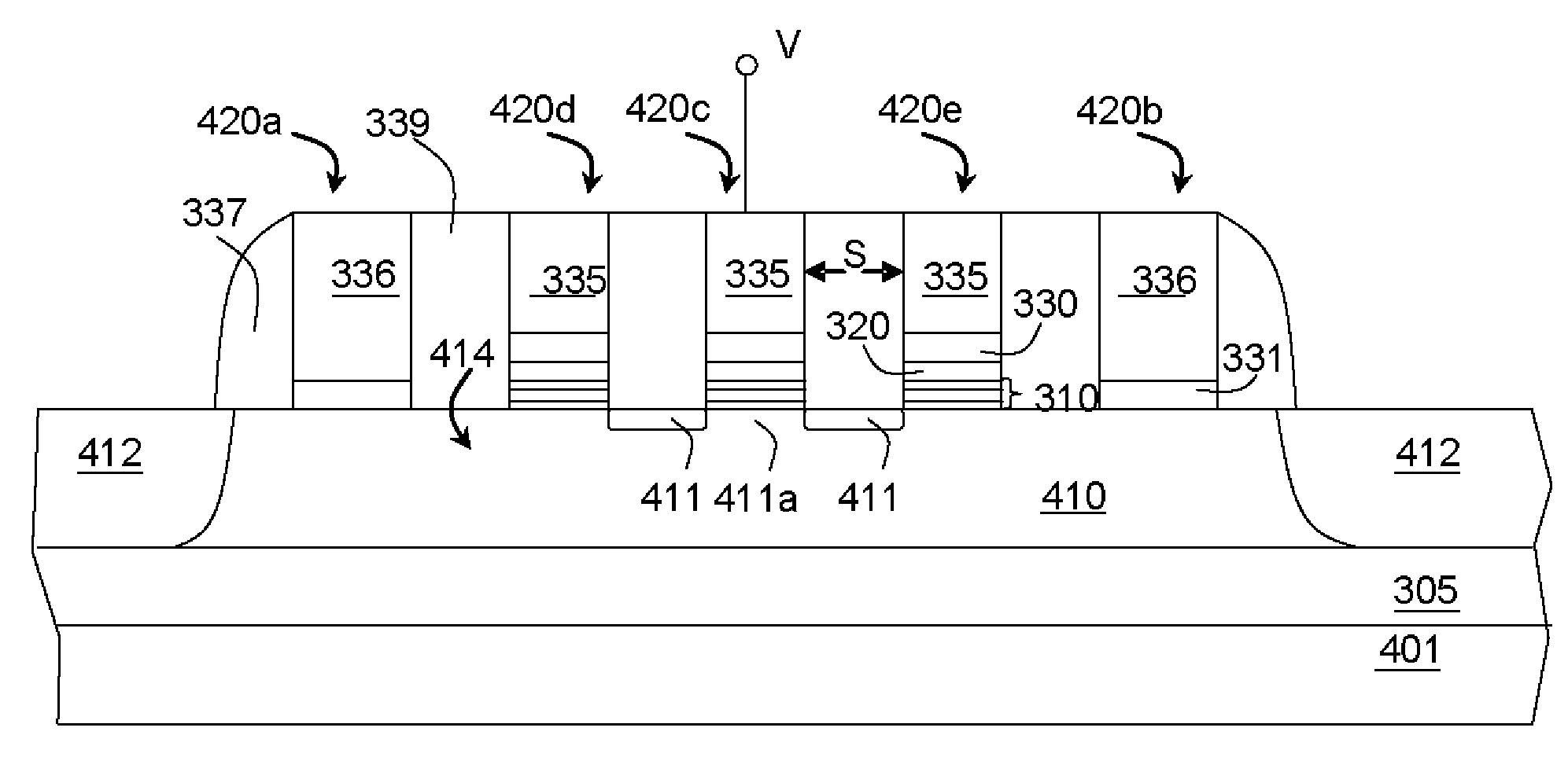
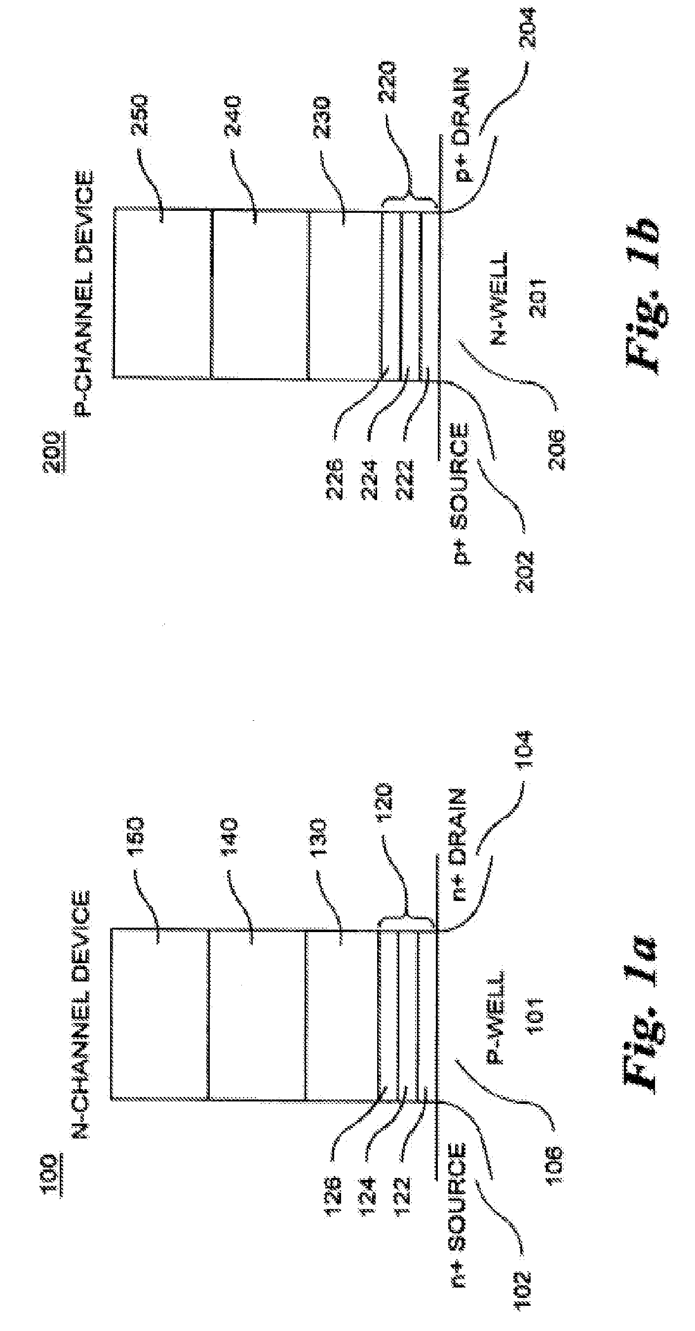
[0104]Reference will now be made in detail to the invention and the presently preferred embodiments thereof, examples of which are illustrated in the accompanying drawings. Wherever possible, the same or similar reference numbers are used in the drawings and the description to refer to the same or like parts. It should be noted that the non-graph drawings are in greatly simplified form and are not to precise scale. In reference to the disclosure herein, for purposes of convenience and clarity only, directional terms, such as top, bottom, left, right, up, down, above, below, beneath, rear, and front, are used with respect to the accompanying drawings. Such directional terms used in conjunction with the following description of the drawings should not be construed to limit the scope of the invention in any manner not explicitly set forth in the appended claims. Although the disclosure herein refers to certain illustrated embodiments, it is to be understood that these embodiments are p...


PUM


Abstract

Memory cells comprising thin film transistor, stacked arrays, employing bandgap engineered tunneling layers in a junction free, NAND configuration. The cells comprise a channel region in a semiconductor strip formed on an insulating layer; a tunnel dielectric structure disposed above the channel region, the tunnel dielectric structure comprising a multilayer structure including at least one layer having a hole-tunneling barrier height lower than that at the interface with the channel region; a charge storage layer disposed above the tunnel dielectric structure; an insulating layer disposed above the charge storage layer; and a gate electrode disposed above the insulating layer Arrays and methods of operation are described.

Description

CROSS-REFERENCE TO RELATED APPLICATIONS[0001]The present application is a continuation-in-part of U.S. patent application Ser. No. 11 / 831,594, filed 31 Jul. 2007; which is a continuation of U.S. patent application Ser. No. 11 / 324,581, filed Jan. 3, 2006, which is based upon, and claims priority under 35 U.S.C. § 119(e) of provisional U.S. Patent Application No. 60 / 640,229, filed on Jan. 3, 2005; provisional U.S. Patent Application No. 60 / 647,012, filed on Jan. 27, 2005; provisional U.S. Patent Application No. 60 / 689,231, filed on Jun. 10, 2005; and provisional U.S. patent application No. 60 / 689,314, filed on Jun. 10, 2005; the entire contents of each of which are incorporated herein by reference.[0002]The present application is a continuation-in-part of U.S. patent application Ser. No. 11 / 425,959, which claims priority to provisional U.S. Patent Application No. 60 / 748,807, filed on Dec. 9, 2005, the entire contents of each of which are incorporated herein by reference.[0003]The pres...

Claims


Application Information

Patent Timeline
IPC IPC(8): G11C11/34H01L21/336
CPCG11C16/0483G11C16/0491H01L21/28282H01L27/115H01L27/11568H01L29/66833H01L27/11551G11C16/0466H01L27/11529H01L27/11578H01L27/11531H01L27/11524H01L29/792H01L29/40117H10B69/00H10B43/30H10B41/20H10B41/35H10B41/41H10B41/42H10B43/20
Inventor LUE, HANG-TINGLAI, ERH-KUN
Owner MACRONIX INT CO LTD
Why Eureka
Try Eureka