
Method for manufacturing a semiconductor device

a manufacturing method and semiconductor technology, applied in semiconductor/solid-state device manufacturing, basic electric elements, electric devices, etc., can solve the problems of slow diffusion, lowering the hf concentration in the hollow portion, reducing the yield, and avoiding the acceleration of etching a si layer. , the effect of reducing the concentration of nitrous acid and etched products

Inactive Publication Date: 2008-07-24
TOKYO INST OF TECH +1
View PDF14 Cites 6 Cited by
  • Summary
  • Abstract
  • Description
  • Claims
  • Application Information

AI Technical Summary

Benefits of technology

[0005]An advantage of the present invention overcomes the above issues and is to provide a method of manufacturing a semiconductor device in which acceleration of etching a Si layer is avoided at the time of etching a SiGe layer.

Problems solved by technology

In this conventional SBSI method, however, the etching ratio of the SiGe layer to the Si layer was deteriorated if it takes long time to selectively etch only the SiGe layer among multiple layers such as Si, SiGe and Si layers.
Such deterioration unintentionally accelerates etching of the Si layer at the time of removing the SiGe layer, facing difficulty in forming stable configuration and uniform thickness of large area's SOI layers or if it has various configurations, lowering the yield.
This slow diffusion lowers HF concentration in the hollow portion and easily increases concentration of nitrous acid and etched products.

Method used


Image

  • Method for manufacturing a semiconductor device
  • Method for manufacturing a semiconductor device
  • Method for manufacturing a semiconductor device

Examples


first embodiment

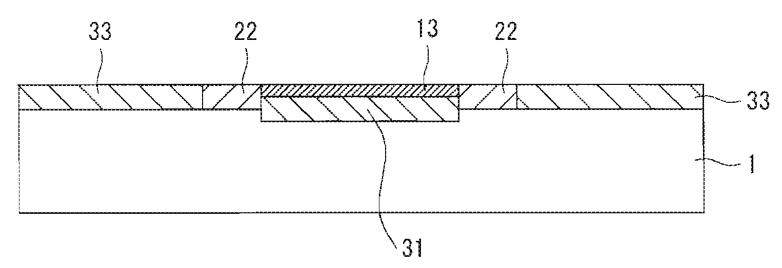
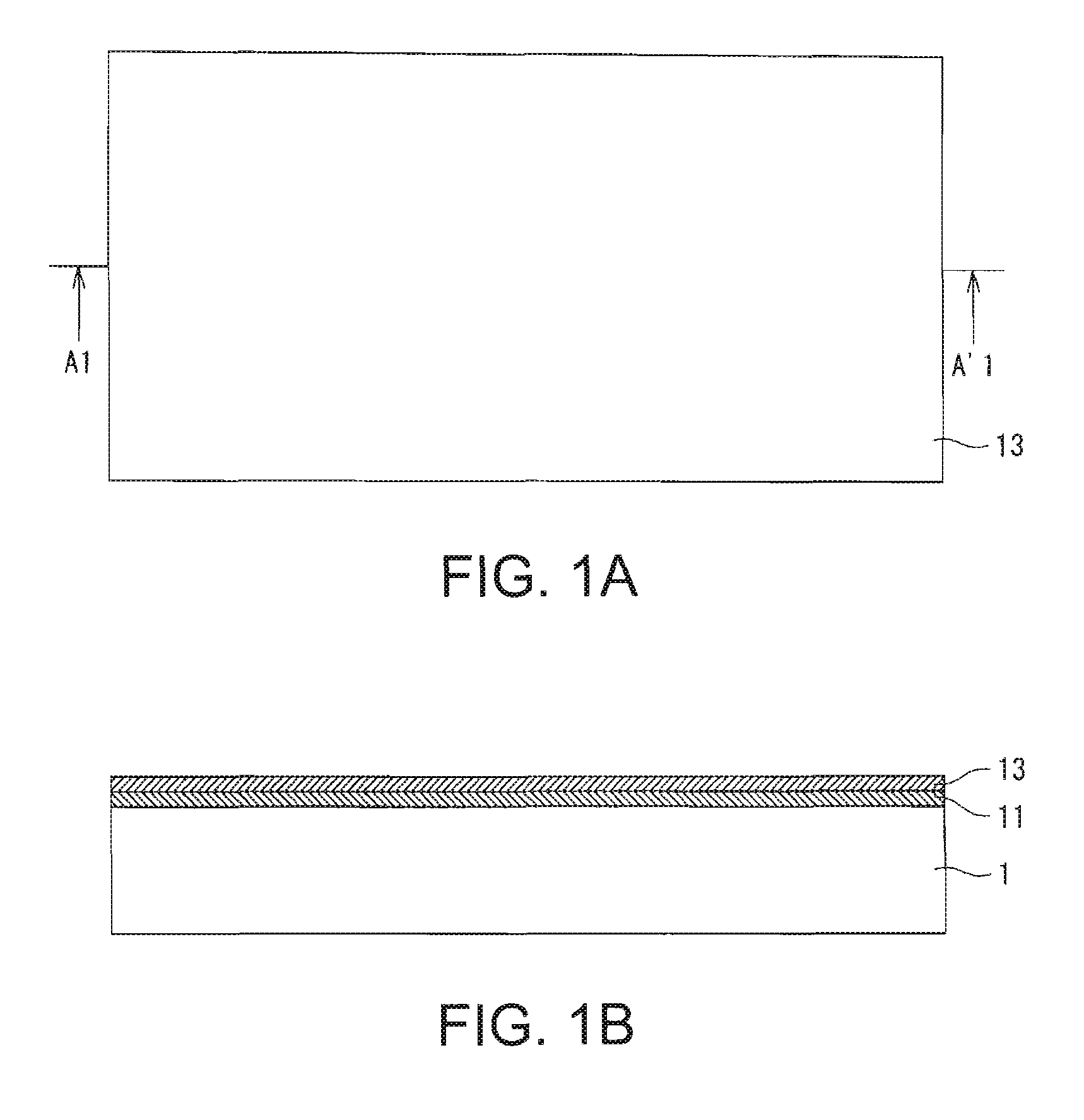
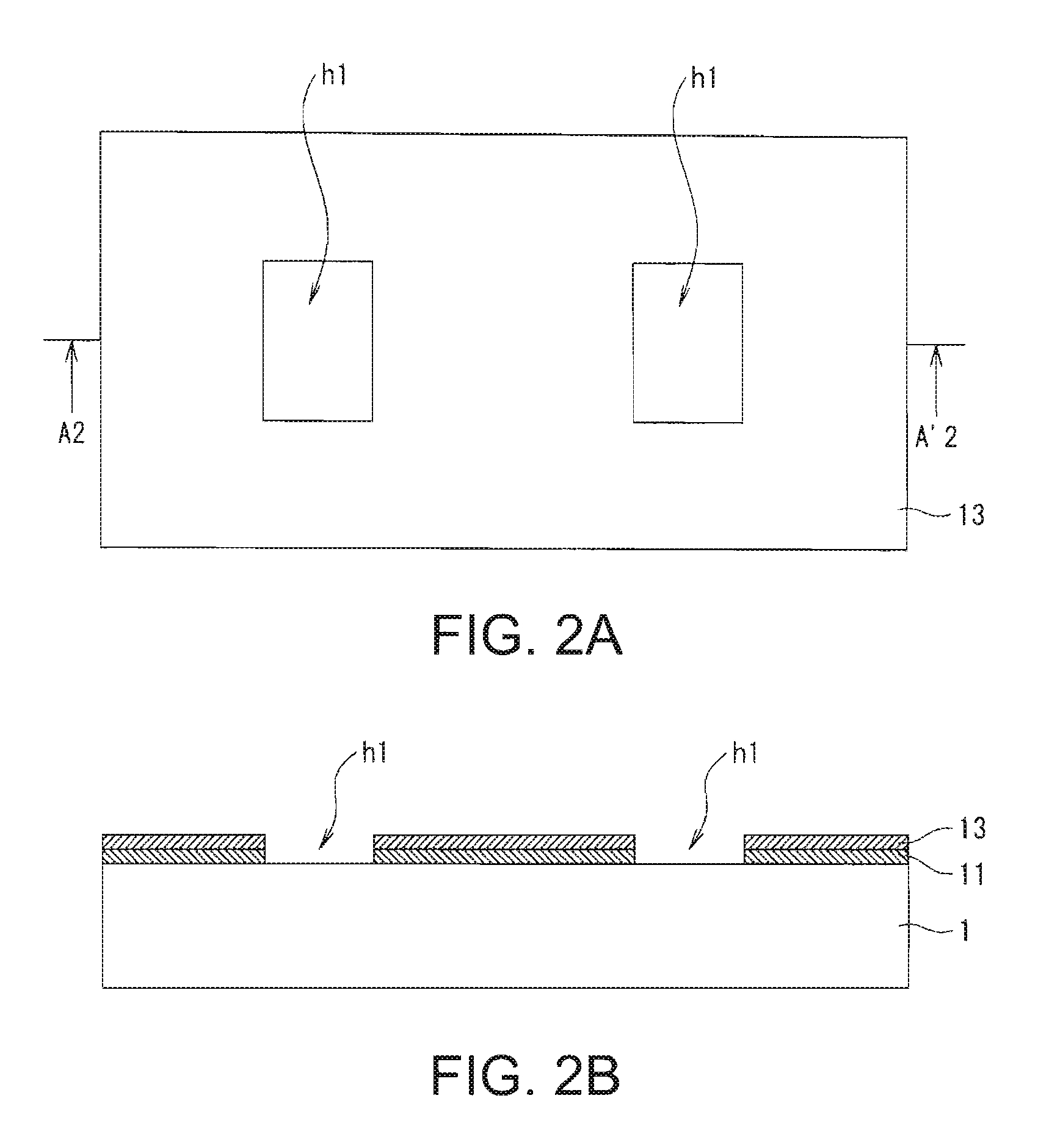
[0032]FIGS. 1 to 7 are view s showing a method for manufacturing a semiconductor device according to an embodiment of the invention. FIG. 1A to FIG. 7A are plain views and FIG. 1B to FIG. 7B are cross sections crossing each of line A-A40 to line A7-A′7 in FIG. 1A to FIG. 7A. FIG. 4C to FIG. 6C are cross sections crossing each of line B4-B′4 to line B6-B6′ in FIG. 4A to FIG. 6A.

[0033]In the embodiment, the SBSI method is applied to the present invention. When the SOI structure is formed by the SBSI method, Si and SiGe layers are formed on a Si substrate 1 and a hollow portion is formed between the Si substrate 1 and the Si layer by selectively removing only the SiGe layer using different etching rate between Si and SiGe. Then, Si exposed in the hollow portion is thermally oxidized, embedding a SiO2 layer between the Si substrate 1 and the Si layer and forming a BOX layer between the Si substrate 1 and the Si layer. Such SBSSI method will be explained.

[0034]Namely, in FIG. 1A and FIG....

second embodiment

[0047]FIGS. 9A and 9C show procedures of selective etching (dipping type) of the SiGe layer 11. Here, as examples of dipping type wet etching, three methods (A) to (C) will be explained. Namely, the wet etching device shown in FIG. 9A comprises an etching chamber 51, a rinsing chamber 52 and a dryer 53. The fluorinated nitric acid solution is stored in the etching chamber 51 and pure water is stored in the rinsing chamber 52. Further, the etching chamber 51 includes a circulating line not shown in the figure, which circulates the fluorinated nitric acid solution, and a filter in the circulating line for filtering impurities and foreign materials.

[0048]In FIG. 9A, the Si substrate 1 is dipped into the fluorinated nitric acid solution stored in the etching chamber 51 and the SiGe layer is wet-etched. Next, the Si substrate 1 is taken out of the etching chamber 51 after one minute later. Then, the Si substrate 1 is dipped into pure water stored in the rinsing chamber 52 and rinsed. Nex...


PUM


Abstract

A method of manufacturing a semiconductor device, comprises; a) forming a SiGe layer on a substrate; b) forming a Si layer on the SiGe layer ; c) forming a groove that exposes the side surface of the SiGe layer by partly etching the Si layer and the SiGe layer; and d) forming a hollow portion between the substrate and, the Si layer by etching the SiGe layer via the groove. Step d) further comprises: forming a part of the hollow portion by supplying a new liquid including a fluorinated nitric acid solution to the substrate and etching the SiGe layer, removing the fluorinated nitric acid solution once from the hollow portion that is under formation; and etching the SiGe layer by refilling a new liquid including a fluorinated nitric acid solution to the hollow portion.

Description

BACKGROUND OF THE INVENTION[0001]1. Technical Field[0002]The present invention relates to a method of manufacturing a semiconductor device, in particular, a method of improving selection ratio of materials such as Si and Ge at the time of etching.[0003]2. Related Art[0004]The utility of a field effect transistor formed on a SOI substrate is brought to an attention because of easiness for isolating elements, latch up free and small source and drain contact capacitance. In particular, a perfect depletion SOI transistor has the capability of fast driven operation with low power consumption and is easily driven by low voltage, enhancing active research for driving SOI transistors with the prefect depletion mode. “Separation Bonding SI Islands (SBSI) for LSI application,” Second International SiGe Technology and Device meeting, Meeting Abstract, pp. 230 to 231, May 2004 written by T. Sakai et al. discloses a method (SBSI method) in which a SOL layer is formed on a bulk substrate to reduc...

Claims


Application Information

Patent Timeline
IPC IPC(8): H01L21/20
CPCH01L21/30604H01L21/187
Inventor KATO, JURIOHMI, SHUNICHIRO
Owner TOKYO INST OF TECH
Learn More