Method for fabrication of a conductive bump structure of a circuit board

a technology of conductive bumps and circuit boards, which is applied in the direction of resist details, non-metallic protective coating applications, double resist layers, etc., can solve the problems of increasing the quantity of electrical connection pads on the carried components, unable to meet the demands for chip development, and shrinking the total area, so as to reduce achieve the effect of reducing material costs, fast electroplating speed, and reducing the difficulty of electroplating

Active Publication Date: 2008-07-31
PHOENIX PRECISION TECH CORP
View PDF2 Cites 14 Cited by
  • Summary
  • Abstract
  • Description
  • Claims
  • Application Information

AI Technical Summary

Benefits of technology

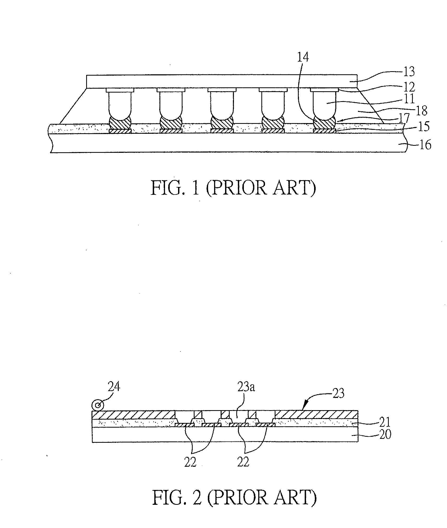
[0011]In light of the above prior art drawbacks, a primary objective of the present invention is to provide a conductive bump structure of the circuit board and a method for fabricating the same to avoid problems related to formation of conductive bumps of uneven height on a surface of the circuit board, so as to ensure the reliability of the subsequent electrical connecting process for circuit boards and external electronic components.
[0012]Another objective of the present invention is to provide a conductive bump structure of the circuit board and a method for fabricating the same to avoid problems such as having the difficulty of electroplating increased due to minimal area for electroplating.
[0013]Still another objective of the present invention is to provide a conductive bump structure of the circuit board and a method for fabricating the same to reduce the amount of solder materials used and the cost of production.

Problems solved by technology

But the change also shrinks the total area of carried components in a chip, which in turn increases the quantity of electrical connection pad on the carried components; as a result, the demands for the development of chip can only be satisfied by shrinking the size and the pitch of electrical connection pad.
But the shrinking of electrical connection pad also makes the openings on the stencil used in stencil printing technology smaller as well.
As a result, the smaller openings on the stencil not only increases the cost for producing the stencil, which is resulted from difficulty in stencil production; but also hampers the later production process because the smaller opening on the stencil can be impervious to the solder material.
Furthermore, apart from the requirement of accurate size of stencil in order to ensure the precision in the shaping of solder material; there are the problems of the number of times the stencil has been used and cleaned.
Since the solder material is viscous, it can stick to the inner wall of openings in the stencil and accumulate as the stencil is used to print many times, and this can give rise to incorrect quantity and shape of solder material from the design specification when the stencil is used next time.
Therefore, when the stencil is put to actual usage, it must be cleaned after a certain times of printing, otherwise problems like conflicting shape and size of solder material can arise and result in the production process being impeded, which lowers its reliability.
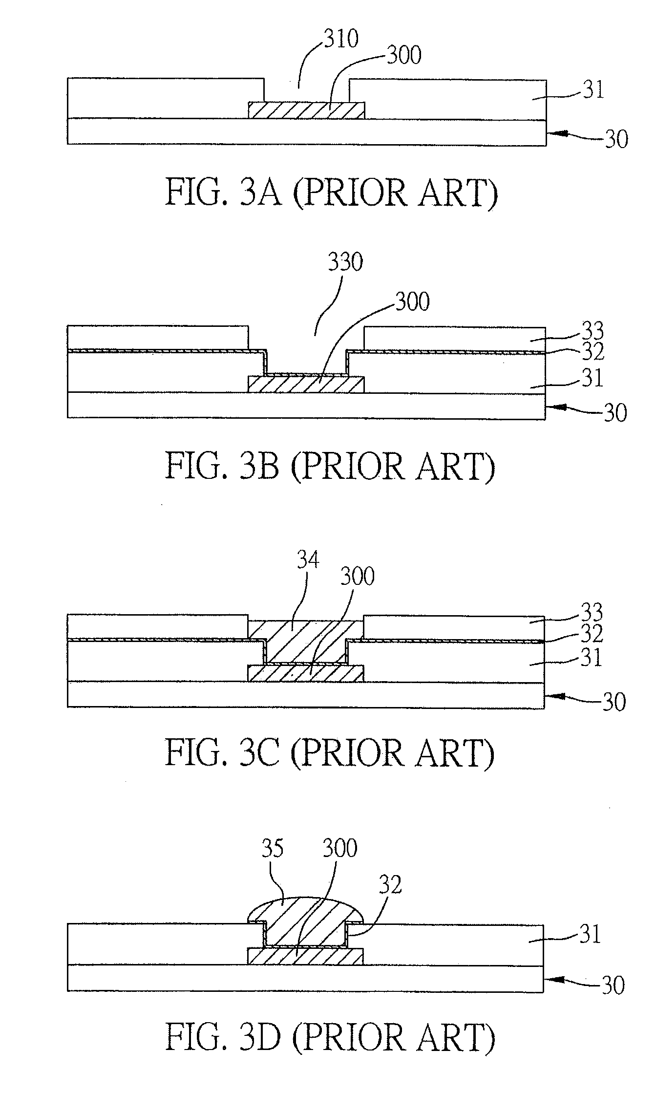
Although the above procedures can solve the problems of stencil printing described previously, the difficulty of electroplating can be increased due to minimal area for electroplating, because solder materials 34 is formed in the openings of resist layer by direct electroplating.
Moreover, when solder material is formed on the electrical connection pads in the openings of solder mask layer by direct electroplating, it becomes difficult to control the height of solder material on the electrical connection pads, which can lead to problems like uneven height of conductive bumps on the surface of circuit board, and this will have serious impact on the reliability of the electrical connecting process of later circuit boards and external electronic components (especially semiconductor chips).

Method used


Image

  • Method for fabrication of a conductive bump structure of a circuit board
  • Method for fabrication of a conductive bump structure of a circuit board
  • Method for fabrication of a conductive bump structure of a circuit board

Examples


Embodiment Construction

[0028]The present invention relates generally to a method for fabricating conductive bump structure of a circuit board, and more particularly, to a conductive bump structure formed on an electrical connection pad of a circuit board for electrically connecting the circuit board to the external electronic component. The following description is presented to enable one of ordinary skill in the art to make and use the invention and is provided in the context of a patent application and its requirements. Various modifications to the preferred embodiments and the generic principles and features described herein will be readily apparent to those skilled in the art. Thus, the present invention is not intended to be limited to the embodiments shown, but is to be accorded the widest scope consistent with the principles and features described herein.

[0029]Proposed in the present invention can be more fully understood by reading the detailed description of the preferred embodiments. What needs ...


PUM

PropertyMeasurementUnit
conductiveaaaaaaaaaa
insulatingaaaaaaaaaa
electrical connectivityaaaaaaaaaa

Abstract

A method for fabricating a conductive bump structure of a circuit board is disclosed. The circuit board with a plurality of electrical connection pads is provided. An insulating protective layer and a resist layer are successively applied on the circuit board, wherein openings are formed in the layers at positions corresponding to the pads to expose the pads. Then, a conductive layer is formed on surfaces of the resist layer and openings, and a metal layer is formed on the conductive layer via electroplating and filled in the openings. Subsequently, the metal layer and conductive layer formed on the resist layer are removed via thinning, so as to form metal bumps on the pads. After the resist layer is removed, the metal bumps are covered by an adhesive layer to form a conductive bump structure for electrically connecting the circuit board to the external electronic component.

Description

CROSS-REFERENCE TO RELATED APPLICATIONS[0001]This application is a divisional application and claims benefit of priority under 35 USC § 121 of U.S. patent application Ser. No. 11 / 370,724, filed Mar. 7, 2006, and under 35 USC 119 of Taiwan Application No. 094107081, filed on Mar. 9, 2005, all of which is incorporated herein by reference.FIELD OF THE INVENTION[0002]The present invention relates to a method for fabricating a conductive bump structure of a circuit board, and more particularly, to a conductive bump structure formed on an electrical connection pad of a circuit board for electrically connecting the circuit board to the external electronic component.BACKGROUND OF THE INVENTION[0003]The flip chip packaging technology was introduced by IBM in the early 1960s, and this technology differs from the wire bonding technology in that the electrical connectivity between the semiconductor chip and the substrate is achieved by the solder bumps instead of the ordinary wires. The main ad...

Claims


Application Information

Patent Timeline
Patent Type & Authority Applications(United States)
IPC IPC(8): C25D5/02
CPCH01L21/4853H01L23/49811H01L2924/10253H01L2224/73204H01L2224/32225H01L2224/136H05K2203/0577H05K2203/054H01L24/81H01L2224/114H01L2224/11462H01L2224/1147H01L2224/116H01L2224/16225H01L2224/81193H01L2224/8121H01L2224/81815H01L2924/01078H01L2924/01079H05K3/0035H05K3/243H05K3/28H05K3/4007H05K2201/0367H05K2201/09845H01L2924/014H01L2924/00H01L2924/14H01L2224/05573H01L2224/05568H01L2924/00014H01L2224/0554H01L2224/05599H01L2224/0555H01L2224/0556
Inventor HU, WEN-HUNG
Owner PHOENIX PRECISION TECH CORP
Why Eureka
Try Eureka